Formation method of lead frame structure

A lead frame and lead structure technology, applied in electrical components, semiconductor/solid-state device manufacturing, circuits, etc., can solve problems such as unfavorable electrical connection of semiconductor chips, high lead frame process cost, and poor lead frame shape. The effect of good morphology and structure, good appearance and stable electrical connection performance

Active Publication Date: 2014-08-06
NANTONG FUJITSU MICROELECTRONICS
View PDF4 Cites 9 Cited by
  • Summary
  • Abstract
  • Description
  • Claims
  • Application Information

AI Technical Summary

Problems solved by technology

[0004] However, in the package structure, the process cost of forming the lead frame is high and the process is difficult, and the shape of the lead frame is poor, which is not conducive to the electrical connection of the semiconductor chip

Method used


Image

  • Formation method of lead frame structure
  • Formation method of lead frame structure
  • Formation method of lead frame structure

Examples


Embodiment Construction

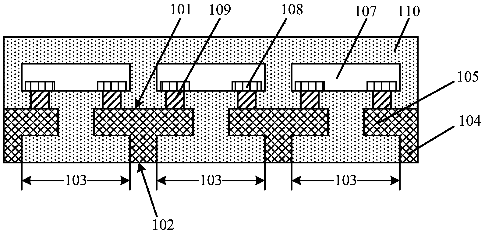
[0032] As mentioned in the background, in the package structure, the process cost of forming the lead frame is high and the process is difficult, and the shape of the lead frame is poor, which is not conducive to the electrical connection of the semiconductor chip.

[0033] After research, it was found that due to figure 1The lead frame shown is formed by etching the provided metal substrate, so the amount of metal material used is relatively large, which increases the process cost of the lead frame. Moreover, since it is more difficult to etch the metal substrate, the process difficulty of the lead frame is increased. In addition, the lead frame formed by etching the metal substrate has poor morphology, which has an adverse effect on the stability of the electrical connection of the semiconductor chip.

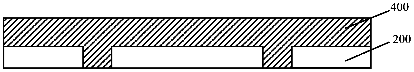
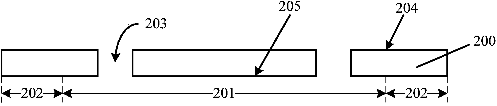
[0034] Specifically, in one embodiment, the forming process of the lead frame includes: providing a metal substrate, the metal substrate has a first surface and a second sur...


PUM


Abstract

Provided is a formation method of a lead frame structure. The formation method of the lead frame structure comprises the steps that a plastic package layer is formed, wherein the plastic package layer is provided with a plurality of supporting areas and cutting areas between the supporting areas, the supporting areas are internally provided with a plurality of first openings penetrating through the plastic package layer, and the plastic package layer is provided with a first surface and a second surface opposite to the first surface; an insulation layer is formed on the first surface of the plastic package layer, wherein the insulation layer is internally provided with second openings exposing the first openings, the second openings are greater than the first openings in size, and the second openings further expose part of the surface, around the first openings in the supporting areas, of the plastic package layer; the first openings and the second openings are filled with conductive materials, and pin structures are formed in the first openings and the second openings, wherein the insulation layer exposes the first surfaces of the pin structures, and the plastic package layer exposes the second surfaces of the pin structures. The process for forming the lead frame is simplified, cost is lowered, and the shape and the electric connection performance of the formed lead frame structure are improved.

Description

technical field [0001] The invention relates to the technical field of semiconductor manufacturing, in particular to a method for forming a lead frame structure. Background technique [0002] With the development of electronic products such as mobile phones and notebook computers towards miniaturization, portable, ultra-thin, multimedia and low-cost to meet the needs of the public, high-density, high-performance, high-reliability and low-cost packaging forms and their Assembly technology has been rapidly developed. Compared with expensive BGA (BallGrid Array) and other packaging forms, new packaging technologies that have developed rapidly in recent years, such as Quad Flat No-lead Package (QFN, Quad Flat No-leadPackage), due to its good thermal performance and electrical The advantages of performance, small size, low cost and high productivity have triggered a new revolution in the field of microelectronic packaging technology. [0003] figure 1 It is a schematic cross-s...

Claims


Application Information

Patent Timeline
Patent Type & Authority Applications(China)
IPC IPC(8): H01L21/48
CPCH01L21/4814H01L21/4885
Inventor 石磊陶玉娟
Owner NANTONG FUJITSU MICROELECTRONICS
Why Eureka
Try Eureka