Organic light-emitting display device and manufacture method thereof
A technology for a display device and a manufacturing method, which is applied in semiconductor/solid-state device manufacturing, electrical components, electric solid-state devices, etc., and can solve problems such as reduced utilization of white light and color mixing of display screens
- Summary
- Abstract
- Description
- Claims
- Application Information
AI Technical Summary
Problems solved by technology
Method used
Image
Examples
Embodiment 1
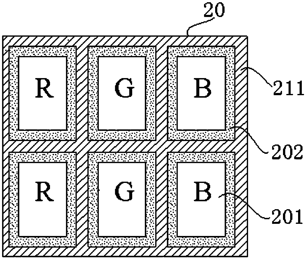
[0019] image 3 is a top view of an organic light emitting display device according to an embodiment of the present invention, Figure 4 for image 3 Schematic diagram of the cross-sectional structure of the organic light-emitting display device along the A-A' section. like image 3 As shown, the organic light-emitting display device according to Embodiment 1 of the present invention includes an array substrate 20, and a plurality of pixel light-emitting regions 201 defined by a pixel definition layer (not shown in the figure) are arranged in a matrix on the array substrate 20, and each A grid 202 is arranged around the pixel light emitting area 201 , and the grid 202 surrounds each pixel light emitting area 201 . A black matrix 211 for light shielding is also provided between the pixels.
[0020] like Figure 4 As shown, the array substrate 20 includes a substrate 203, and a thin film transistor driving layer 204 is arranged on the substrate 203. The thin film transistor...
Embodiment 2
[0029] Figure 5 It is a schematic structural diagram of an organic light-emitting display device in this embodiment; Image 6 for Figure 5 Schematic diagram of the cross-sectional structure of the organic light-emitting display device along the B-B' section. like Figure 5 As shown, the organic light-emitting display device according to Embodiment 2 of the present invention includes an array substrate 20, and a plurality of pixel light-emitting regions 201 defined by a pixel definition layer (not shown in the figure) are arranged in a matrix on the array substrate 20, and each A grid 202 is arranged around the pixel light emitting area 201 , and the grid 202 surrounds each pixel light emitting area 201 . A black matrix 211 for light shielding is also provided between the pixels.
[0030] like Image 6 As shown, the array substrate 20 includes a substrate 203, and a thin film transistor driving layer 204 is arranged on the substrate 203. The thin film transistor driving ...
Embodiment 3
[0038] This embodiment specifically describes the manufacturing method of the organic light emitting display device in the above two embodiments.
[0039] like Figure 7a As shown, a substrate 203 is provided, and a glass substrate can be used. A thin film transistor driving layer 204 is formed on the substrate 203. The thin film transistor driving layer 204 specifically includes thin film transistor switches, data lines and gate lines (not shown in the figure), and is used to control the display of the organic light emitting device. Wherein, the thin film transistor switch (TFT, thin film transistor) may use low-temperature polysilicon or oxide semiconductor TFT.
[0040] Next, if Figure 7b As shown, a conductive layer such as indium tin oxide-silver-indium tin oxide composite layer (ITO-Ag-ITO) is deposited on the thin film transistor driving layer 204 , the conductive layer is patterned, and a reflective electrode 205 is formed by wet etching. The reflective electrode c...
PUM
 Abstract
Description
Claims
Application Information
 - R&D
- Intellectual Property
- Life Sciences
- Materials
- Tech Scout
- Unparalleled Data Quality
- Higher Quality Content
- 60% Fewer Hallucinations
Browse by: Latest US Patents, China's latest patents, Technical Efficacy Thesaurus, Application Domain, Technology Topic, Popular Technical Reports.
© 2025 PatSnap. All rights reserved.Legal|Privacy policy|Modern Slavery Act Transparency Statement|Sitemap|About US| Contact US: help@patsnap.com


