

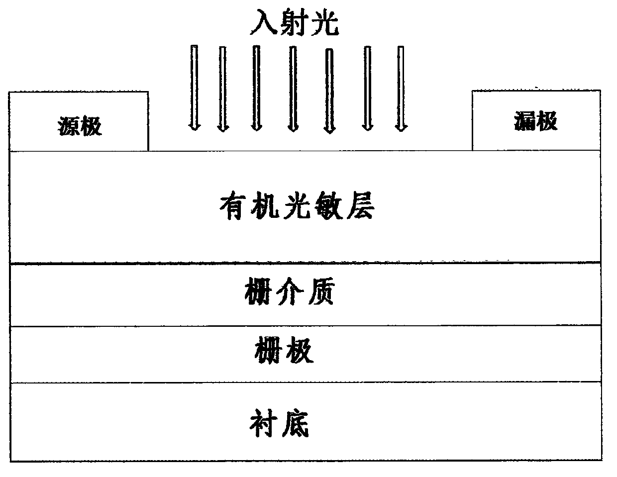
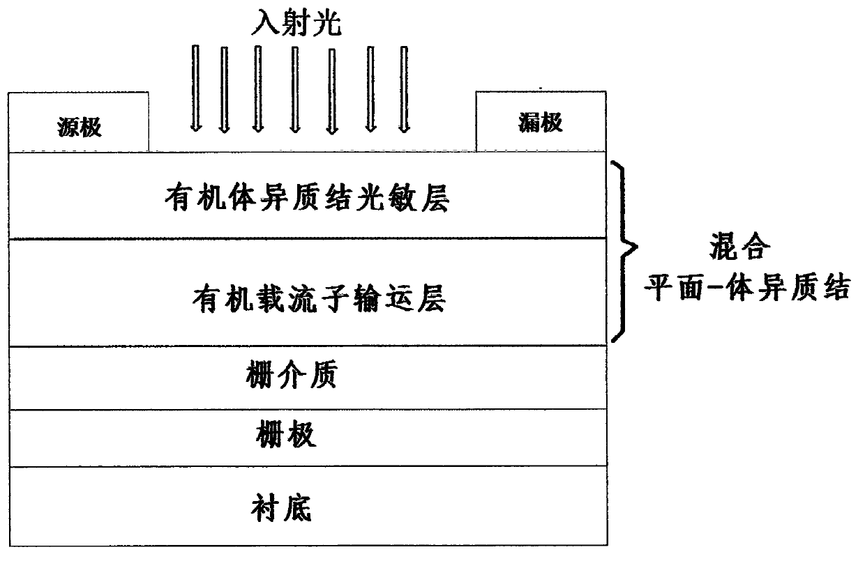
Mixed plane-bulk heterojunction photosensitive organic field effect transistor
A bulk heterojunction, organic field technology, applied in photovoltaic power generation, electric solid state devices, semiconductor devices, etc., can solve the performance limitations of photosensitive organic field effect transistors and other problems
- Summary
- Abstract
- Description
- Claims
- Application Information
AI Technical Summary
Problems solved by technology
Method used
Image

Examples
Embodiment Construction
[0009] to n + -Si / SiO 2 It is the gate / gate dielectric and also serves as the substrate, copper phthalocyanine (CuPc) is the organic carrier transport layer, palladium phthalocyanine (PdPc): C60 (1:1) is the organic isocyanine Taking the photosensitive layer as an example, the preparation process of the present invention is as follows:
[0010] a) Clean with standard process n + -Si / SiO 2 Substrate;
[0011] b) by vacuum evaporation method in n + -Si / SiO 2 Prepare a layer of copper phthalocyanine film on it;
[0012] c) A bulk heterojunction film of PdPc:C60 (1:1) was prepared on the copper phthalocyanine film by vacuum evaporation. The length of the channel and the area of the source and drain electrodes are defined by a mask.
[0013] d) Prepare high work function metal Au as drain and source by vacuum evaporation method.
[0014] The above description is for carrying out the present invention and its embodiments. Those skilled in the art can determine various im...
PUM
 Abstract
Description
Claims
Application Information