

Multiple quantum well structure and growth method thereof, and LED chip having the structure
A multi-quantum well structure, LED chip technology, applied in electrical components, circuits, semiconductor devices, etc., can solve problems such as low luminous efficiency of LED chips
- Summary
- Abstract
- Description
- Claims
- Application Information
AI Technical Summary
Problems solved by technology
Method used
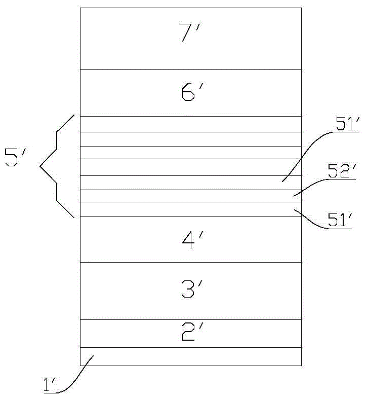
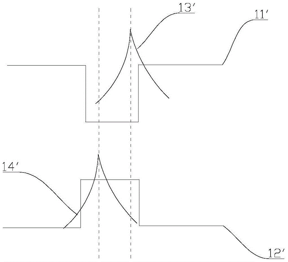
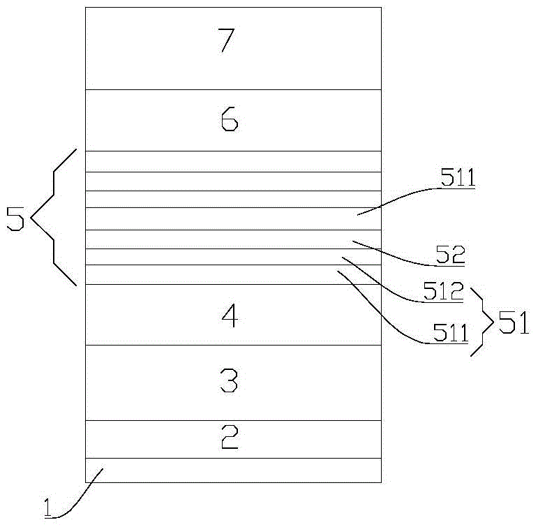
Image

Examples
Embodiment 1
[0050] The preparation method of the LED chip containing the multi-quantum well structure:
[0051] 1. The hydrogen atmosphere pressure in the reaction chamber is maintained at 150mbar and the sapphire substrate is processed at 1200°C for 10 minutes;
[0052] 2. Lower the temperature to 650°C, maintain the pressure of the reaction chamber at 600mbar, and grow a low-temperature buffer layer GaN with a thickness of 50nm on the sapphire substrate;
[0053] 3. Raise the temperature to 1200°C, maintain the pressure in the reaction chamber at 300mbar, and continue to grow 4μm undoped GaN;
[0054] 4. Then continue to grow N-type GaN doped with Si, the Si doping concentration is 1E+19, and the total thickness is controlled at 4 μm;
[0055] 5. Growth of multi-quantum well structure: (1) The pressure of the reaction chamber is maintained at 400mbar, the low temperature is 750°C, and NH with a flow rate of 60000sccm is introduced at the same time 3 , TEGa with a flow rate of 150 sccm...
Embodiment 2
[0060] The preparation method of the LED chip containing the multi-quantum well structure:
[0061] 1. The hydrogen atmosphere pressure in the reaction chamber is maintained at 100mbar to process the sapphire substrate at 1000°C for 5 minutes;
[0062] 2. Lower the temperature to 550°C, maintain the pressure of the reaction chamber at 400mbar, and grow a low-temperature buffer layer GaN with a thickness of 20nm on the sapphire substrate;
[0063] 3. Raise the temperature to 1000°C, maintain the pressure of the reaction chamber at 150mbar, and continue to grow 2μm undoped GaN;
[0064] 4. Then continue to grow N-type GaN doped with Si, the Si doping concentration is 5E+18, and the total thickness is controlled at 2 μm;
[0065] 5. Growth of multi-quantum well structure: (1) The pressure of the reaction chamber is maintained at 300mbar, the low temperature is 700°C, and NH with a flow rate of 50000sccm is introduced at the same time 3 , TEGa with a flow rate of 100 sccm. The ...
Embodiment 3
[0070] The preparation method of the LED chip containing the multi-quantum well structure:
[0071] 1. The hydrogen atmosphere pressure in the reaction chamber is maintained at 130mbar and the sapphire substrate is processed at 1100°C for 6 minutes;
[0072] 2. Lower the temperature to 570°C, maintain the pressure of the reaction chamber at 500mbar, and grow a low-temperature buffer layer GaN with a thickness of 40nm on the sapphire substrate;
[0073] 3. Raise the temperature to 1100°C, maintain the pressure in the reaction chamber at 180mbar, and continue to grow 3μm undoped GaN;
[0074] 4. Then continue to grow N-type GaN doped with Si, the Si doping concentration is 8E+18, and the total thickness is controlled at 3 μm;
[0075] 5. Growth of multi-quantum well structure: (1) The pressure of the reaction chamber is maintained at 350mbar, the low temperature is 740°C, and NH with a flow rate of 55000sccm is introduced at the same time 3 , TEGa with a flow rate of 140 sccm....
PUM
 Abstract
Description
Claims
Application Information