Large chip for LED lighting

A technology of LED lighting and LED chips, which is applied in the direction of lighting devices, lighting and heating equipment, components of lighting devices, etc., and can solve the problems of small area of ​​LED chips and related circuits, small batches of manufacturers, thick optical-mechanical templates, etc. , to achieve the effect of facilitating standardized operations, simple production process, and short production process

Active Publication Date: 2014-08-13
GUIZHOU GUANGPUSEN PHOTOELECTRIC
View PDF13 Cites 21 Cited by
  • Summary
  • Abstract
  • Description
  • Claims
  • Application Information

AI Technical Summary

Problems solved by technology

The problem of using the optomechanical template as an epitaxial wafer to directly grow chips is that the optomechanical template has 7 specifications, and each specification has a variety of power requirements, and producers will face the embarrassing problem of too many varieties and small batches; Secondly, the area occupied by the LED chip and related circuits is relatively small compared to the area of ​​the optical-mechanical template, and the production cost remains high; moreover, the optical-mechanical template is thicker than the substrate, which also relatively increases the cost.

Method used


Image

  • Large chip for LED lighting
  • Large chip for LED lighting
  • Large chip for LED lighting

Examples


Embodiment Construction

[0045] The present invention will be further described below in conjunction with the drawings and embodiments, but it is not a basis for limiting the present invention.

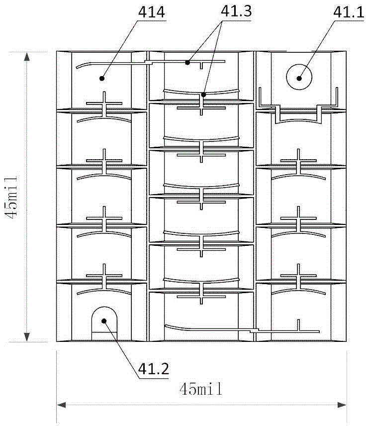
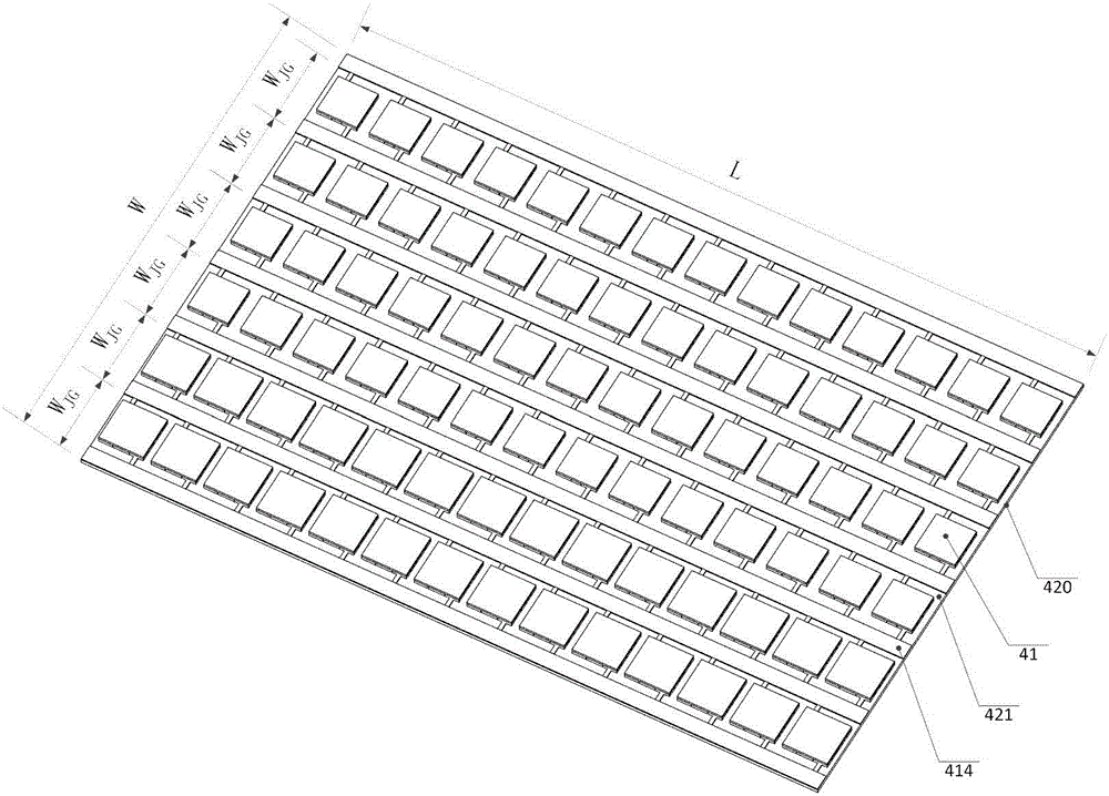
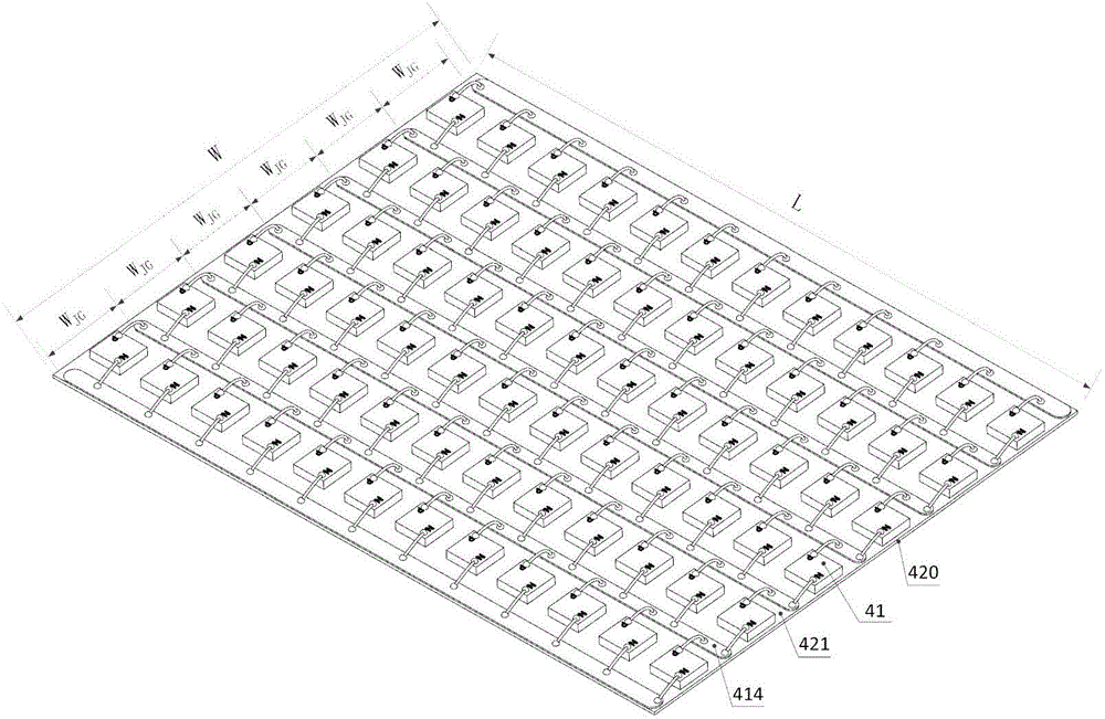
[0046] Examples. LED lighting chip, such as Figure 1 to 3 Shown: It includes a first transparent substrate 421 with a fixed width of W. N+1 parallel interface wires are provided on the first transparent substrate 421, and N LED chips 41 are provided on the first transparent substrate 421 to form a series of LED chips. Group, each LED chip 41 is located between two adjacent interface wires, and the distance between two adjacent interface wires is W JG Equal to W minus the interface wire width and then divided by N(W JG =(W-interface wire width) / N), and the positive and negative poles of each LED chip 41 are respectively connected to two adjacent interface wires; and multiple LED series groups are connected in parallel at the same time, so that the first transparent substrate 421 An array of N columns and multi...


PUM


Abstract

The invention discloses a large chip for LED lighting. The large chip comprises a first transparent substrate (421) with a fixed width W, N+1 parallel interface wires are arranged on the first transparent substrate (421), LED chip series connection sets formed by N LED chips (41) are arranged on the first transparent substrate (421), each LED chip (41) is located between two adjacent interface wires, the distance between the two adjacent interface wires is WJG, wherein the WJG=(W-the with of the interface wire) / N, and the positive pole and the negative pole of each LED chip (41) are respectively connected to the two adjacent interface wires. Meanwhile, the multiple LED series connection sets are in series connection, so that an N-column and multi-row LED chip array capable of extending in the length direction of the first transparent substrate (421) is formed in the first transparent substrate (421), wherein N is an integer ranging from 3 to 7.

Description

Technical field [0001] The invention relates to a large LED lighting chip, which belongs to the technical field of LED lighting. Background technique [0002] Chinese patent applications such as 201310140124.5, 201310140138.7, 201310140150.8, 201310140105.2, 201310140134.9, 201310140106.7, 201310140151.2, 201310140136.8 and other Chinese patent applications disclose a number of optical-mechanical module technical solutions that can be used on universal and interchangeable LED bulbs. These technologies have laid the foundation for the establishment of a lighting industry architecture centered on LED bulbs, and the basic concept of making LED bulbs (lighting sources), lamps, and lighting control become independent production and application end products. However, the above-mentioned patents have not yet solved the problem of the built-in drive power of the optical-mechanical module. [0003] The current LED driving power supplies are mostly switching power supplies, which are too bu...

Claims


Application Information

Patent Timeline
Patent Type & Authority Applications(China)
IPC IPC(8): H01L33/48H01L25/075H01L33/62H01L25/16H05B37/02F21S2/00F21V3/04F21Y101/02F21K9/00F21Y105/16F21Y115/10
CPCF21V19/001F21Y2101/00F21Y2105/10F21Y2115/10H01L25/13H01L33/62H05B47/10
Inventor 张继强张哲源朱晓冬
Owner GUIZHOU GUANGPUSEN PHOTOELECTRIC
Why Eureka
Try Eureka