
Metal Al monocrystal film growing on sapphire substrate and preparing method and application of metal Al monocrystal film

A sapphire substrate and single crystal thin film technology, which is applied in semiconductor/solid-state device manufacturing, electrical components, circuits, etc., can solve the problems of poor performance such as the purity of metal Al thin films, crystal quality and surface flatness, and achieve repeatability , easy access, high crystal quality results

Active Publication Date: 2014-08-20
广州市众拓光电科技有限公司
View PDF3 Cites 2 Cited by
  • Summary
  • Abstract
  • Description
  • Claims
  • Application Information

AI Technical Summary

Problems solved by technology

[0005] In order to solve the poor performance problems such as the purity of the existing metal Al thin film, crystal quality and surface flatness, the present invention provides a kind of low-cost, high-quality metal Al single crystal grown on the sapphire substrate Thin film and its preparation method and application

Method used


Image

  • Metal Al monocrystal film growing on sapphire substrate and preparing method and application of metal Al monocrystal film
  • Metal Al monocrystal film growing on sapphire substrate and preparing method and application of metal Al monocrystal film
  • Metal Al monocrystal film growing on sapphire substrate and preparing method and application of metal Al monocrystal film

Examples


Embodiment 1

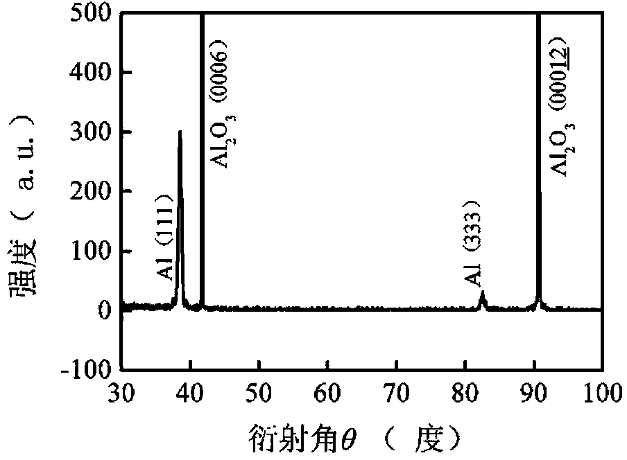
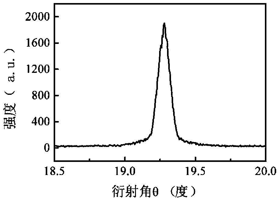
[0033] A metal Al single crystal film grown on a sapphire substrate, including Al 2 o 3 The substrate 11 and the metal Al single crystal thin film 12 grown in the direction of the epitaxial direction (0002) to the (10-12) plane by 0.2°. The thickness of the metal Al single crystal thin film is 350nm.

[0034] The metal Al single crystal film grown on the sapphire substrate is prepared by the following steps:

[0035] a. Al 2 o 3 The substrate is cleaned and annealed; the specific process of the annealing is: the substrate is placed in the annealing chamber, and the Al 2 o 3 The substrate is annealed for 60 minutes and then cooled to room temperature in air; the cleaning is specifically: Al 2 o 3 Substrates were placed in deionized water and then ultrasonically cleaned at room temperature for 3 minutes to remove Al 2 o 3 The dirt particles on the surface of the substrate are washed with hydrochloric acid, acetone, and ethanol in sequence to remove surface organic matte...

Embodiment 2

[0043] A metal Al single crystal thin film grown on a sapphire substrate comprises an Al2O3 substrate and a metal Al single crystal thin film whose (0002) plane deviates 0.4° to the (10-12) direction for epitaxial growth. The thickness of the metal Al single crystal thin film is 420nm.

[0044] The metal Al single crystal film grown on the sapphire substrate is prepared by the following steps:

[0045] a. Clean and anneal the Al2O3 substrate; the specific process of the annealing is: put the substrate into the annealing chamber, and treat the Al2O3 substrate in an air atmosphere at 870°C 2 o 3 The substrate is annealed for 60 minutes and then cooled to room temperature in air; the cleaning is specifically: Al 2 o 3 The substrate was placed in deionized water, and then ultrasonically cleaned at room temperature for 3 minutes to remove Al 2 o 3 The dirt particles on the surface of the substrate are washed with hydrochloric acid, acetone, and ethanol in sequence to remove su...


PUM

PropertyMeasurementUnit
thicknessaaaaaaaaaa
thicknessaaaaaaaaaa
thicknessaaaaaaaaaa

Abstract

The invention relates to a metal Al monocrystal film growing on a sapphire substrate. The metal Al monocrystal film growing on the sapphire substrate comprises an Al2O3 substrate and a metal Al monocrystal film body, wherein the AlN metal Al monocrystal film body grows in an epitaxial mode from the face (0002) of the Al2O3 substrate to the direction deviating from the face (10-12) by 0.2 to 0.5 degree. The invention further relates to a preparing method of the metal Al monocrystal film. The method is characterized by including the following steps that a, the Al2O3 substrate is cleaned and annealed; b, the direction from the face (0002) of the Al2O3 substrate treated through the step a to the direction deviating from the face (10-12) by 0.2 to 0.5 degree serves as the epitaxial growth direction of crystal and the metal Al monocrystal film body grows in the epitaxial mode. The metal Al monocrystal film is used for preparing a photoelectric device or an optical multilayer film and is low in cost, high in quality and wide in application range.

Description

technical field [0001] The invention relates to a metal Al single crystal film and its preparation method and application, in particular to a metal Al single crystal film grown on a sapphire substrate and its preparation method and application. Background technique [0002] With the advent of the first transistor in 1950, all fields of science and technology have undergone great changes due to the development of solid-state electronics. For more than half a century, people have higher and higher requirements on the structure size and performance of microelectronic components. In the 1940s, the size of vacuum components was still on the centimeter level. In the 1960s, the size of solid components was developed to the millimeter level. In the 1980s, the size of components in VLSI was only microns. class size. In the 21st century, people have higher requirements for electronic components, and the size of molecular electronic components will be as small as nanometers. In the ...

Claims


Application Information

Patent Timeline
Patent Type & Authority Applications(China)
IPC IPC(8): H01L21/20H01L21/268H01L33/32H01L31/0352
CPCH01L21/02697H01L33/405H01L33/46
Inventor 李国强
Owner 广州市众拓光电科技有限公司
Learn More