Panel structure and making method thereof
A manufacturing method and panel technology, applied to semiconductor devices, electrical components, circuits, etc., can solve problems such as reduced process yield, damage to display components, and long process time, so as to reduce costs, reduce release force, and improve process yield. rate effect
- Summary
- Abstract
- Description
- Claims
- Application Information
AI Technical Summary
Problems solved by technology
Method used
Image

Examples
Embodiment Construction
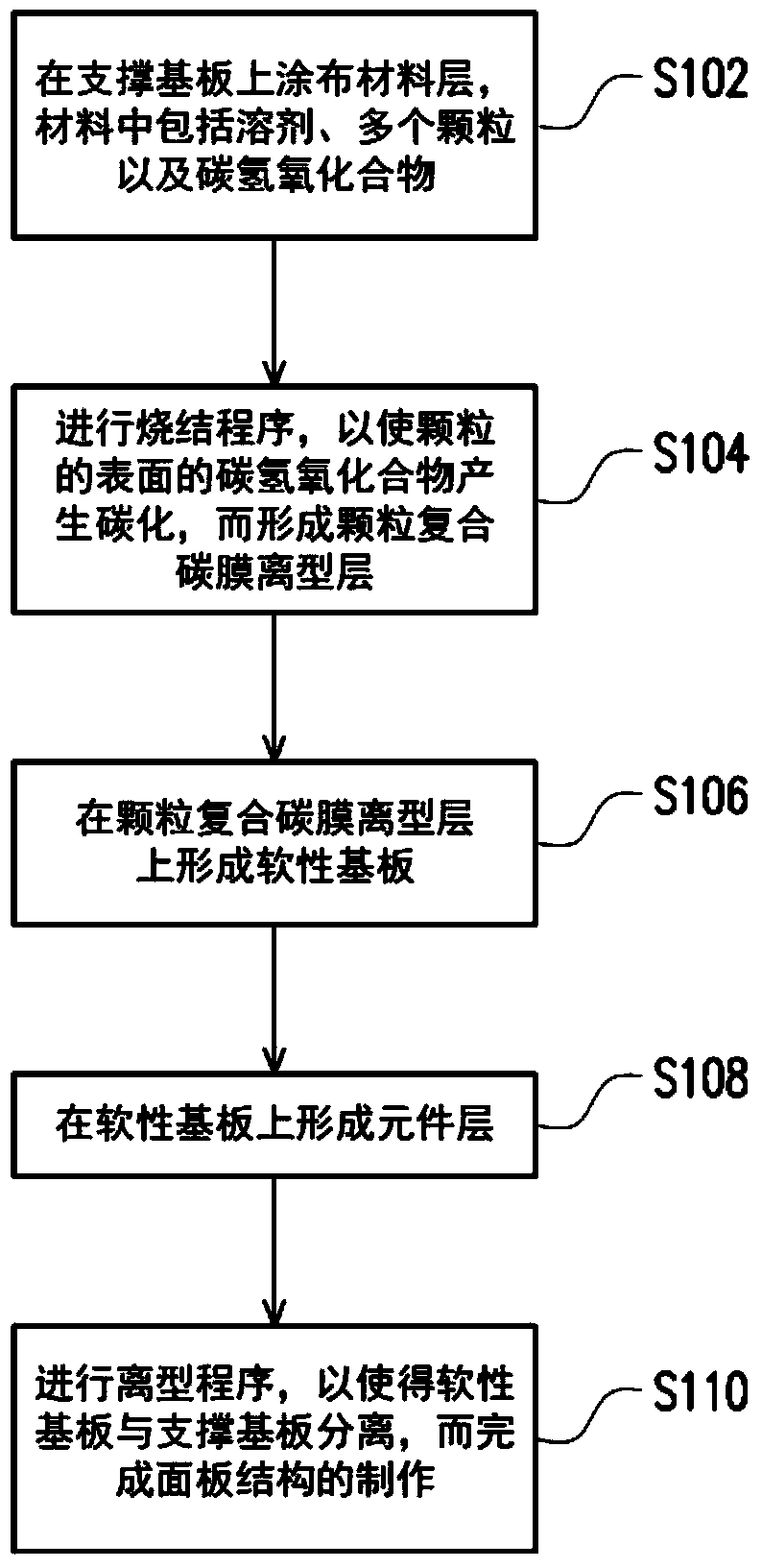
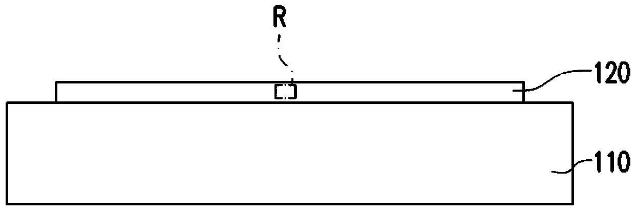
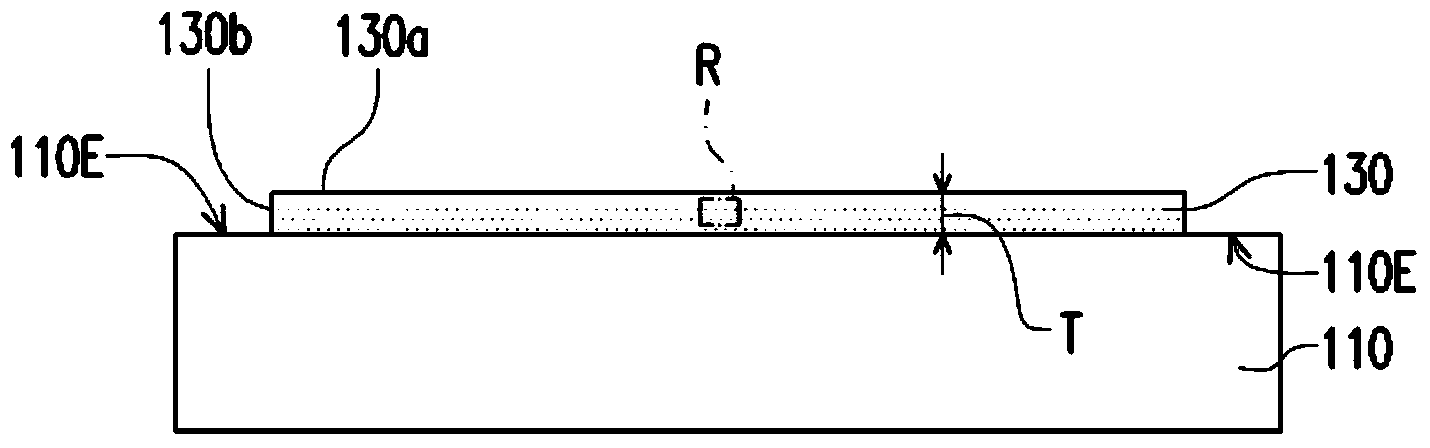
[0054] figure 1 It is a flowchart of a manufacturing method of a panel structure according to an embodiment of the present invention, Figure 2A to Figure 2F for figure 1 A schematic cross-sectional view of the fabrication method of the panel structure, while Figure 3A to Figure 3B respectively Figure 2A to Figure 2B An enlarged schematic view of the region R.
[0055] Please also refer to figure 1 Step S102, Figure 2A as well as Figure 3AFirst, the material layer 120 is coated on the support substrate 110 . In more detail, the material layer 120 can be formed on the support substrate 110 by wet coating, wherein the material layer 120 can also be called a coating solution. The supporting substrate 110 may be a substrate having properties of high rigidity, low expansion coefficient, and high Young's modulus. In this embodiment, the supporting substrate 110 is, for example, an inorganic substrate, including a glass substrate, a quartz substrate or a silicon substrate...
PUM
| Property | Measurement | Unit |
|---|---|---|
| Thickness | aaaaa | aaaaa |
| Size | aaaaa | aaaaa |
| Size | aaaaa | aaaaa |
Abstract
Description
Claims
Application Information