
Ceramic Copper Circuit Board And Semiconductor Device Employing Same

A technology for circuit substrates and ceramic substrates, which is applied in semiconductor devices, semiconductor/solid-state device components, and improvement of metal adhesion on insulating substrates.

Active Publication Date: 2014-08-27
KK TOSHIBA +1
View PDF8 Cites 23 Cited by
  • Summary
  • Abstract
  • Description
  • Claims
  • Application Information

AI Technical Summary

Problems solved by technology

Therefore, the restriction on the design of the semiconductor device becomes large.

Method used


Image

  • Ceramic Copper Circuit Board And Semiconductor Device Employing Same
  • Ceramic Copper Circuit Board And Semiconductor Device Employing Same
  • Ceramic Copper Circuit Board And Semiconductor Device Employing Same

Examples


Embodiment 1~11、 comparative example 1~9

[0045] As the ceramic substrate, a silicon nitride substrate with a thickness of 0.635mm (thermal conductivity: 90W / m·K, three-point bending strength: 730MPa) and an aluminum nitride substrate with a thickness of 0.635mm (thermal conductivity: 180W / m·K, three-point bending strength: 400MPa), an alumina substrate with a thickness of 0.635mm (thermal conductivity: 15W / m·K, three-point bending strength: 500MPa). The shape of the ceramic substrate is uniformly 50 mm long x 30 mm wide.

[0046] Next, the active metal solder material having the composition shown in Table 1 was prepared and pasted, and then coated on the ceramic substrate. The coating thickness of the active metal solder paste is shown in Table 1. Next, a copper plate (oxygen-free copper plate) having a thickness of 0.3 mm was prepared. The shape of the copper plates is uniformly 45 mm in length x 25 mm in width. In Examples 1 to 9, a copper plate having a thickness of 0.3 mm was used, and in Examples 10 to 11, a cop...

Embodiment 12~13

[0059] The ceramic copper circuit board of Example 9 was referred to as Example 12, and the ceramic copper circuit board obtained by changing the thickness of the copper plate of the ceramic copper circuit board of Example 9 to 0.5 mm was referred to as Example 13. For the ceramic copper circuit board of Example 12 and Example 13, under condition 2 (1 cycle: -40°C×30 minutes→room temperature (25°C)×10 minutes→175°C×30 minutes→room temperature (25°C)× 10 minutes) TCT was performed, and the number of cycles in which cracks occurred in the ceramic substrate was investigated. The results are shown in Table 4.

[0060] [Table 4]

[0061]

[0062] It can be seen from Table 4 that the ceramic copper circuit board of the example also has a durability of 6000 cycles or more for TCT with a maximum temperature exceeding 170°C.

Embodiment 14~18

[0064] The following substrate was prepared as a ceramic substrate. The ceramic substrate 1 is a silicon nitride substrate with a thickness of 0.320 mm (thermal conductivity: 93 W / m·K, three-point bending strength: 700 MPa). The ceramic substrate 2 is a silicon nitride substrate with a thickness of 0.320 mm (thermal conductivity: 100 W / m·K, three-point bending strength: 600 MPa). The ceramic substrate 3 is an aluminum nitride substrate having a thickness of 0.635 mm (thermal conductivity: 200 W / m·K, three-point bending strength: 320 MPa). The ceramic substrate 4 is an alumina substrate (thermal conductivity: 12 W / m·K, three-point bending strength: 400 MPa) with a plate thickness of 0.635 mm. In addition, the shape of the ceramic substrate is uniformly 50 mm in length × 30 mm in width.

[0065] Next, the active metal solder material of the composition shown in Table 5 was prepared and paste, and printed on the ceramic substrate and applied. A copper plate with a length of 45 mm...


PUM

PropertyMeasurementUnit
strengthaaaaaaaaaa
lengthaaaaaaaaaa
flexural strengthaaaaaaaaaa

Abstract

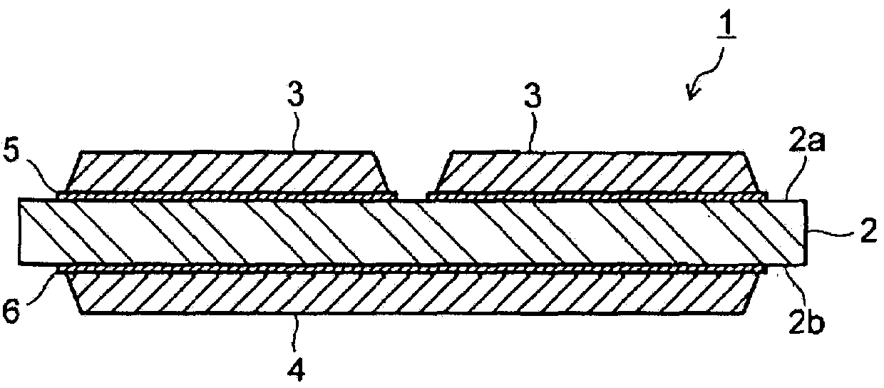
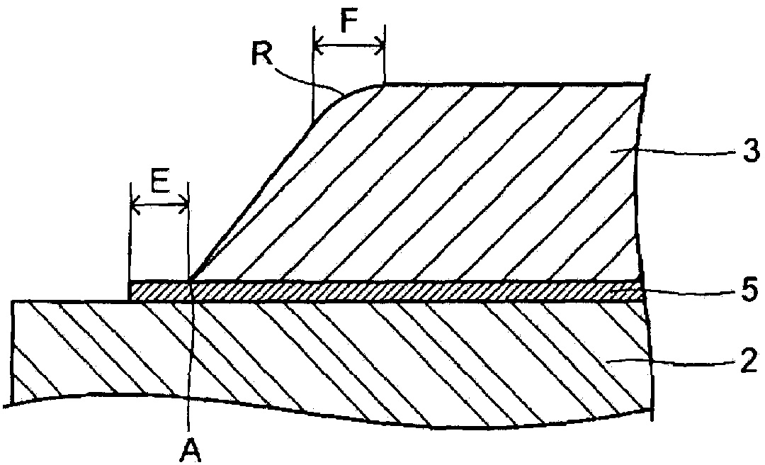
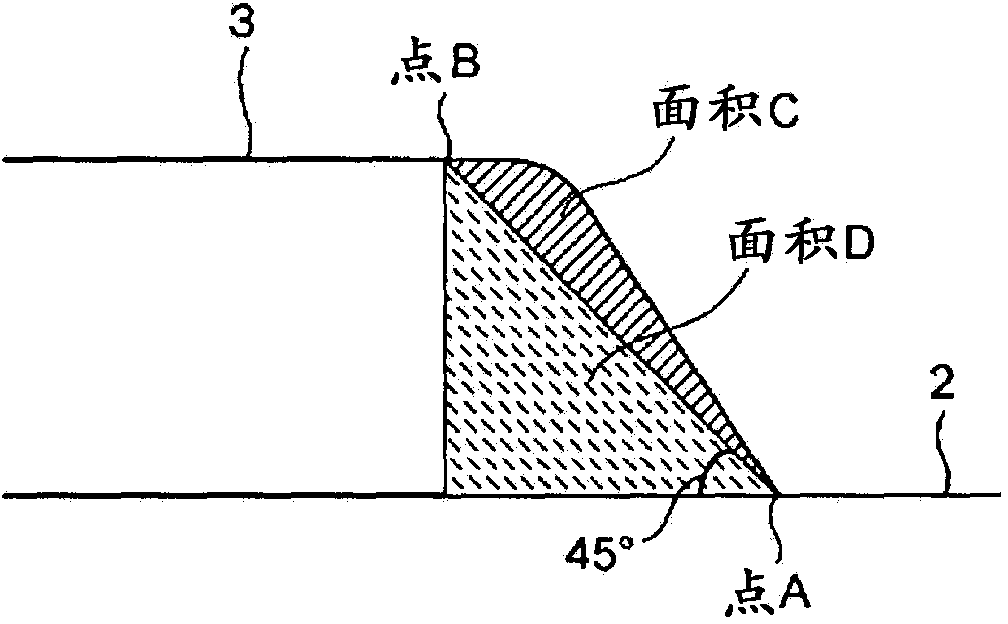
A ceramic / copper circuit board of an embodiment includes a ceramic substrate and first and second copper plates bonded to surfaces of the ceramic substrate via bonding layers containing active metal elements. In cross sections of end portions of the first and second copper plates, a ratio (C / D) of an area C in relation to an area D is from 0.2 to 0.6. The area C is a cross section area of a portion protruded toward an outer side direction of the copper plate from a line AB, and the area D is a cross section area of a portion corresponding to a right-angled triangle whose hypotenuse is the line AB. R-shape sections are provided at edges of upper surfaces of the first and second copper plates, and lengths F of the R-shape sections are 100 μm or less.

Description

Technical field [0001] Embodiments of the present invention relate to a ceramic copper circuit board and a semiconductor device using the ceramic copper circuit board. Background technique [0002] In the past, low-cost aluminum oxide substrates, high thermal conductivity aluminum nitride substrates, high-strength silicon nitride substrates and other ceramic substrates, and high thermal conductivity copper plates and other metal plates have been used for power module circuit boards. (Mo), tungsten (W) high melting point metal method, DBC (Direct Bonding Copper) method using the eutectic reaction of copper and oxygen, active metal using active metal such as titanium (Ti) Bonded substrates obtained by bonding by bonding methods or the like. The metal plate joined to the ceramic substrate is patterned, for example, by etching, thereby constituting a circuit substrate. In various bonding methods, the bonding strength can be improved, so active metal bonding methods are generally us...

Claims


Application Information

Patent Timeline
Patent Type & Authority Applications(China)
IPC IPC(8): H01L23/12C04B37/02H01L23/13H01L23/14H05K1/02H05K1/09
CPCH01L29/1608C04B2237/366H05K1/0306C04B2237/706C04B2237/704C04B2237/88C04B2237/343C04B2237/368H05K1/09C04B37/026C04B2235/96H05K2201/09827C04B2237/86C04B2237/708C04B2237/126H05K3/38H05K2201/098H01L23/3735C04B2237/407C04B2237/127C04B2237/125C04B2235/9607H01L2924/0002Y10T428/24488H05K2201/2009H05K2201/09154H01L2924/00
Inventor 矢野圭一加藤宽正宫下公哉那波隆之
Owner KK TOSHIBA
Learn More