Supercharge Your Innovation With Domain-Expert AI Agents!

Hybrid-structured memory array and method of making the same

A technology of memory array and hybrid structure, applied in semiconductor/solid-state device manufacturing, electric solid-state devices, semiconductor devices, etc., can solve problems such as product cracking, product data tampering, etc., achieve random adjustment of location distribution, increase the scope of application and Market adaptability and the effect of reducing production costs

Active Publication Date: 2016-09-07
INTEGRATED SILICON SOLUTION SHANGHAI
View PDF4 Cites 0 Cited by
  • Summary
  • Abstract
  • Description
  • Claims
  • Application Information

AI Technical Summary

Problems solved by technology

Such a layout allows the product cracker to take some specific measures (such as laser irradiation, temperature control, electrical interference, etc.) for the ROM array or flash memory array, and at the same time monitor the response changes of the entire chip system (such as power consumption, specific circuit timing, etc.) etc.), and then obtain the specific storage location of the key instructions of the microcontroller product operating system (usually stored in the ROM array) or user key information (usually stored in the flash memory array) and the corresponding system response, which may eventually lead to the product being cracked, the product data has been tampered with

Method used


Image

  • Hybrid-structured memory array and method of making the same
  • Hybrid-structured memory array and method of making the same
  • Hybrid-structured memory array and method of making the same

Examples


Embodiment Construction

[0055] In the following description, many technical details are proposed in order to enable readers to better understand the application. However, those skilled in the art can understand that without these technical details and various changes and modifications based on the following implementation modes, the technical solution claimed in each claim of the present application can be realized.

[0056] In order to make the purpose, technical solution and advantages of the present invention clearer, the following will further describe the implementation of the present invention in detail in conjunction with the accompanying drawings.

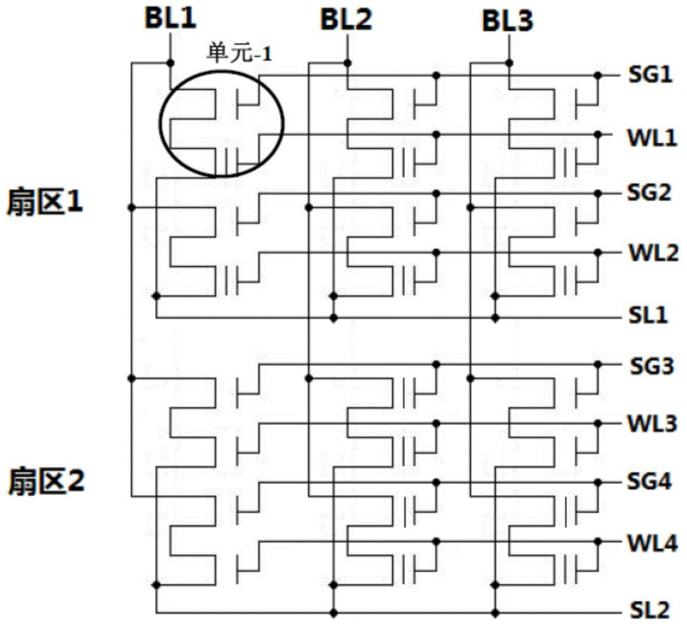
[0057] The first embodiment of the present invention relates to a hybrid structure memory array. figure 1 is a schematic diagram of the memory array of the hybrid structure. The memory array with a hybrid structure includes a flash memory array and a read-only memory (Read-Only Memory, "ROM" for short) array, and the flash memory array and the RO...


PUM


Abstract

The invention relates to the field of semiconductor devices and discloses a hybrid structure memory array and a preparation method thereof. In the hybrid structure memory array of the present invention, the difference between the structure of the ROM cell and the structure of the flash memory cell is only in the channel injection, the connection between the gate and the floating gate, and the presence or absence of electrodes. Only three layers of masks need to be modified, namely 2T pMOS flash memory cells can be converted into ROM cells. Therefore, under the same process and the same area, flash memory arrays and ROM arrays of different capacities can be freely combined, and the appearance of flash memory arrays and ROM arrays is almost the same. , the position distribution can be adjusted at will, which not only significantly reduces production costs, but also greatly increases the product's applicable scope and market adaptability, and effectively improves the product's safety level.

Description

technical field [0001] The invention relates to the field of semiconductor devices, in particular to a memory array with a mixed structure and a preparation method thereof. Background technique [0002] Embedded Flash Memory (Embedded Flash Memory) is usually integrated into a system-level chip in the form of an IP core (Intellectual Property Core, intellectual property core), such as a mobile phone SIM-card (SIM is an abbreviation for Subscriber Identity Module, referring to a customer identification module) chip , Smart bank card chips, etc. Because of this feature, it is called "embedded" to distinguish it from products formed by Stand-alone Flash Memory. [0003] However, the inventors of the present invention have found that existing embedded chips also have the following problems: [0004] 1. The existing embedded flash technology has high complexity (30-40 layers of photomasks) and long production cycle (40-60 days); [0005] 2. Taking bank financial IC card produc...

Claims


Application Information

Patent Timeline
Patent Type & Authority Patents(China)
IPC IPC(8): H01L27/115H01L27/112H01L21/8246H01L21/8247H10B69/00H10B20/00
Inventor 陶凯林志光
Owner INTEGRATED SILICON SOLUTION SHANGHAI
Features
  • R&D
  • Intellectual Property
  • Life Sciences
  • Materials
  • Tech Scout
  • Unparalleled Data Quality
  • Higher Quality Content
  • 60% Fewer Hallucinations
Learn More