Organic electroluminescent display panel, packaging method thereof and display device

An electroluminescence display and display panel technology, which is applied in the directions of organic semiconductor devices, materials and circuits of organic semiconductor devices, can solve the problems of increasing packaging cost and packaging complexity, and achieves increasing packaging cost and packaging complexity, reducing packaging costs and reducing packaging complexity. The effect of lateral water and oxygen erosion area and simple structure

Active Publication Date: 2014-09-10
BOE TECH GRP CO LTD
View PDF4 Cites 30 Cited by
  • Summary
  • Abstract
  • Description
  • Claims
  • Application Information

AI Technical Summary

Problems solved by technology

[0006] The technical problem to be solved by the present invention is how to better avoid the impact of water and oxygen erosion on the OLED device in the OLED device packaging structure without increasing the packaging cost and packaging complexity

Method used


Image

  • Organic electroluminescent display panel, packaging method thereof and display device
  • Organic electroluminescent display panel, packaging method thereof and display device
  • Organic electroluminescent display panel, packaging method thereof and display device

Examples


Embodiment 1

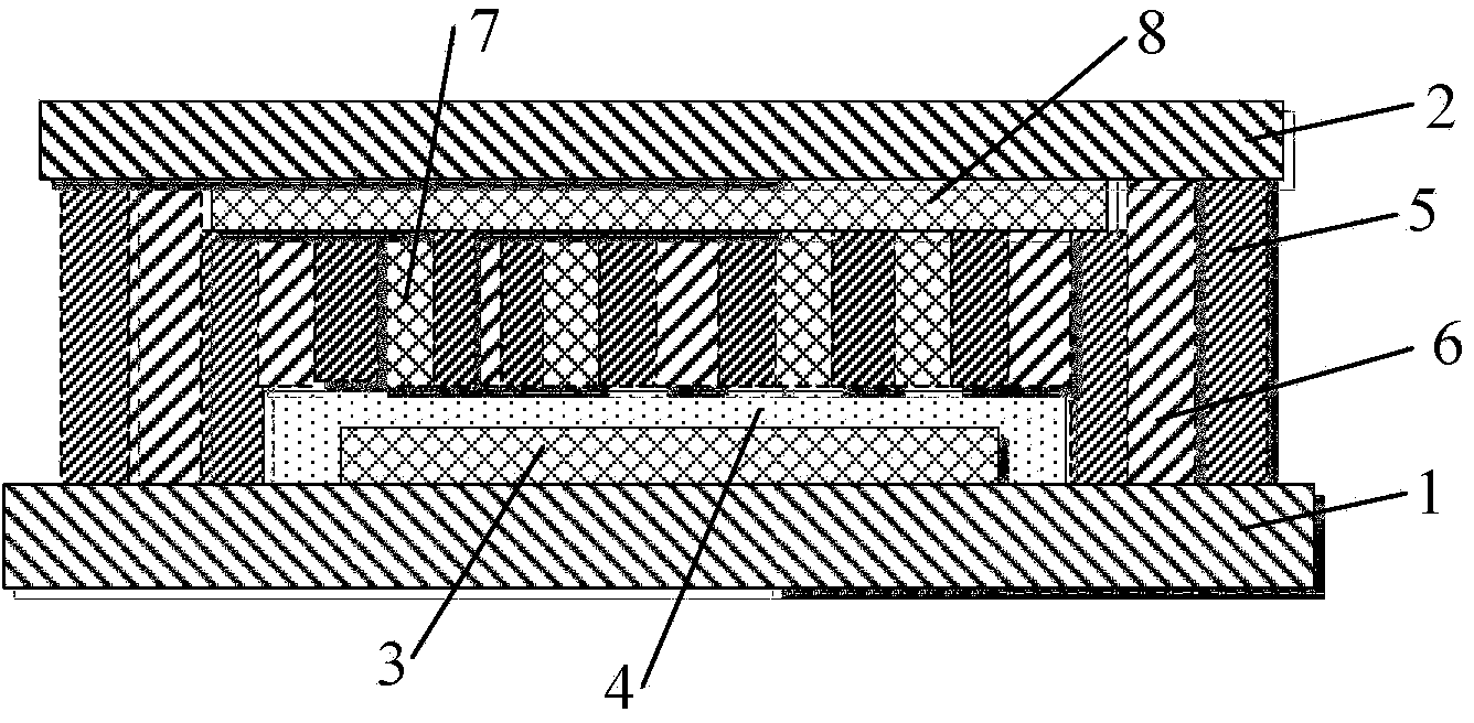
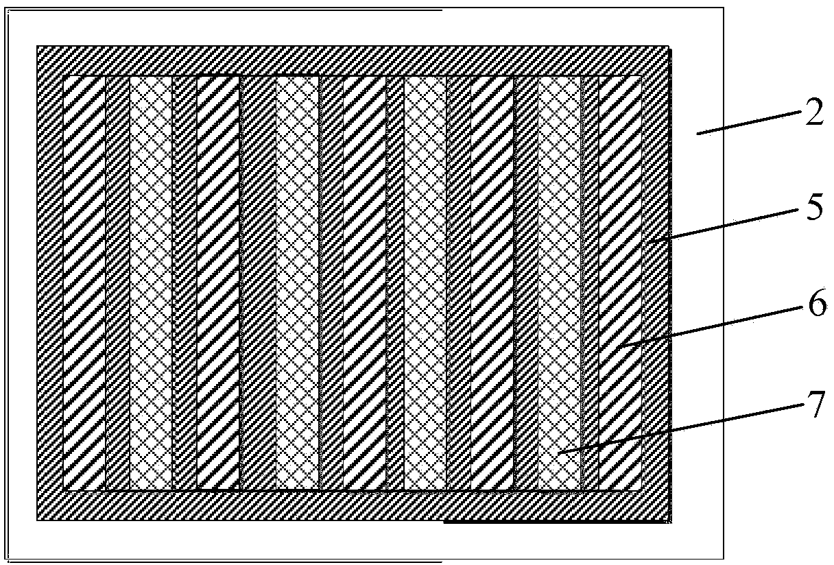
[0034] refer to figure 1 As shown, the organic electroluminescence display panel of this embodiment includes a device substrate 1 and a packaging cover plate 2, the device substrate 1 includes an organic light emitting diode 3, and the organic light emitting diode 3 is covered by a storage cavity 4, and the storage cavity 4 is made of a waterproof material Made to protect the organic light emitting diode 3 from water vapor erosion, and avoid water vapor erosion of the organic light emitting diode 3 in the process of forming other structures in the later stage; an encapsulation protection structure is fabricated between the device substrate 1 and the encapsulation cover plate 2, The packaging protection structure includes multi-layer functional layers that are perpendicular to the device substrate 1 and the packaging cover plate 2 and alternately interspersed. Water layer, it can be understood that the outermost layer described in the embodiment of the present invention means t...

Embodiment 2

[0047] Based on the organic electroluminescent display panel mentioned in Example 1, this example describes the packaging method of this organic electroluminescent display panel. The specific manufacturing steps are as follows: first, prepare the device substrate and packaging cover plate, and Including an organic light emitting diode; then an encapsulation protection structure is formed between the device substrate and the packaging cover plate, the encapsulation protection structure includes a multi-layer functional layer, the multi-layer functional layer is a water blocking layer, and a moisture absorption layer and / or a heat dissipation layer, the function The outermost layer of the layer is a water-blocking layer; each functional layer has multiple layers, and different functional layers are arranged alternately.

[0048] Specifically, in the packaging process of the display panel, a part of the functional layer is firstly formed on the device substrate at intervals, and t...

example 1

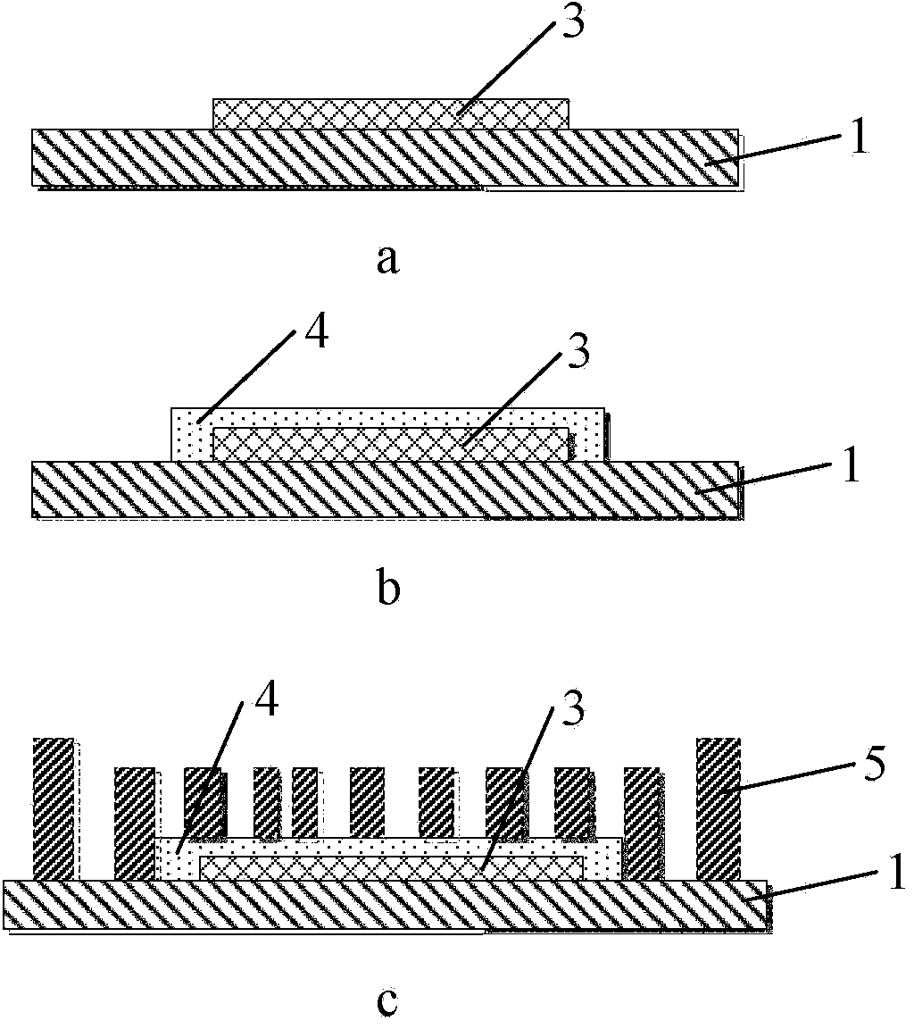
[0051] First, refer to image 3 As shown, an OLED device 3 is sequentially formed on a device substrate 1 ( image 3 As shown in a), the moisture-proof accommodating cavity 4 ( image 3 b), and a multi-layer first functional layer perpendicular to the device substrate 1, wherein the first functional layer is a water blocking layer 5 ( image 3 as shown in c);

[0052] refer to Figure 4 As shown, the buffer layer 8 is sequentially formed on the package cover plate 2 ( Figure 4 a), and the second functional layer perpendicular to the package cover plate 2 ( Figure 4 b) and the third functional layer ( Figure 4 c), wherein the second functional layer is the heat dissipation layer 7, and the third functional layer is the hygroscopic layer 6;

[0053] Secondly, the device substrate and the package cover are pressed together, the moisture absorption layer 6 and the heat dissipation layer 7 are embedded in the gap between the multi-layer water blocking layer 5, and the wate...


PUM


Abstract

The invention discloses an organic electroluminescent display panel, a packaging method thereof and a display device. The organic electroluminescent display panel comprises a device substrate and a packaging cover plate, wherein the device substrate comprises an organic light emitting diode; a packaging protection structure is produced between the device substrate and the packaging cover plate; the packaging protection structure comprises a functional layer which is vertical to the device substrate and the packaging cover plate; the functional layer comprises a waterproof layer, a moisture-absorbing layer and/or a radiating layer; the outermost layer of the functional layer is the waterproof layer. As the functional layer including the waterproof layer is distributed vertically to the device substrate and the packaging cover plate to enable all the functional layers to be arranged in the same layer alternately, the distance between the device substrate and the packaging cover plate can be reduced efficiently, a lateral water oxygen erosion area can be reduced, and heat energy generated by the organic light emitting diode can be emitted out uniformly, rapidly and efficiently; meanwhile, the packaging cost and the packaging complexity cannot be added as the organic electroluminescent display panel is simple in structure, easy and convenient to package.

Description

technical field [0001] The invention relates to the field of display technology, in particular to an organic electroluminescent display panel, a packaging method thereof, and a display device. Background technique [0002] OLED (Organic Light-Emitting Diode, Organic Light-Emitting Diode) devices have become a very Competitiveness and prospects for next-generation display technologies. [0003] The organic light-emitting materials and cathode materials used in OLED devices are particularly sensitive to water and oxygen, and the presence of trace amounts of water and oxygen will often make the device ineffective; at the same time, a large amount of heat will be generated during the light-emitting process and often gather in specific parts. The transfer also has a significant impact on the lifetime of OLED devices. [0004] The existing OLED device packaging structure is to stack the heat dissipation layer, water blocking layer, drying layer (also called moisture absorption l...

Claims


Application Information

Patent Timeline
Patent Type & Authority Applications(China)
IPC IPC(8): H01L51/50H01L51/52H01L51/56H01L27/32
CPCH10K50/846H10K50/8445H10K50/8428H10K50/87H10K2102/00H10K71/00H10K59/00H10K50/80H10K50/00
Inventor 宋文峰罗程远
Owner BOE TECH GRP CO LTD
Why Eureka
Try Eureka