Wave-absorbing magnetic-conductive shielding film and manufacture method thereof

A magnetic shielding and waveguide technology, which is applied in the field of wave-absorbing magnetic shielding film and its production, can solve the problems of secondary electromagnetic pollution, electromagnetic shielding film cannot meet the needs, and the thickness of the shielding film is large

Active Publication Date: 2014-09-10
广州宏庆电子有限公司
View PDF6 Cites 22 Cited by
  • Summary
  • Abstract
  • Description
  • Claims
  • Application Information

AI Technical Summary

Problems solved by technology

[0003] However, the traditional electromagnetic shielding film has the following two defects: first, in terms of raw materials, the selection of shielding materials can realize the shielding effect by reflecting electromagnetic waves, but the reflected electromagnetic waves do not disappear or attenuate, which may cause secondary electromagnetic pollution; Although the selection of wave-absorbing materials can absorb and attenuate electromagnetic waves, it usually only

Method used


Image

  • Wave-absorbing magnetic-conductive shielding film and manufacture method thereof
  • Wave-absorbing magnetic-conductive shielding film and manufacture method thereof
  • Wave-absorbing magnetic-conductive shielding film and manufacture method thereof

Examples


Embodiment 1

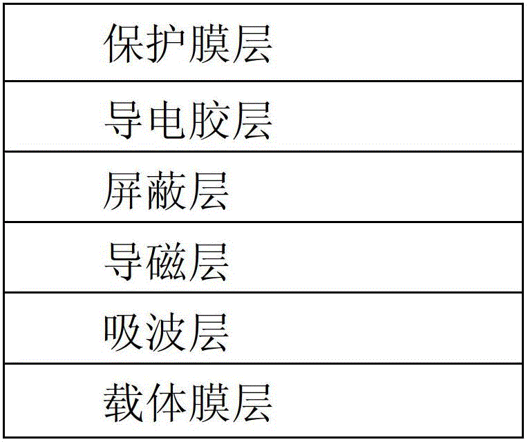
[0059] like figure 1 As shown, the wave-absorbing magnetic shielding film of the present invention includes a carrier film layer 1 , a wave-absorbing layer 2 , a magnetic-conducting layer 3 , a shielding layer 4 , a conductive adhesive layer 5 and a protective film layer 6 from inside to outside.

[0060] 1. Make the carrier film layer:

[0061] 1) Select a PET polyester film with a thickness of 50 μm and a width of 600 mm as the base film layer, and perform corona pretreatment on one side of the film layer. The voltage during the pretreatment process is 20000V, and its surface tension reaches 60 dynes ; Then apply the adhesive layer on the corona-pretreated side surface using ordinary screen printing technology, and dry to form a carrier film layer after coating. The drying temperature is 150°C and the drying time is 50 seconds.

[0062] Wherein, the coating for forming the adhesive layer is selected from epoxy resin and ethyl ester according to the weight ratio of 40:60, an...

Embodiment 2

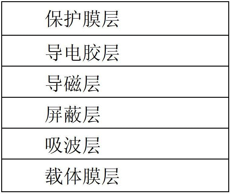
[0092] like figure 1 As shown, the wave-absorbing magnetic shielding film of the present invention includes a carrier film layer 1 , a wave-absorbing layer 2 , a magnetic-conducting layer 3 , a shielding layer 4 , a conductive adhesive layer 5 and a protective film layer 6 from inside to outside.

[0093] 1. Make the carrier film layer:

[0094] 1) Select a PEN polyester film with a thickness of 50 μm and a width of 600 mm as the base film layer, and perform corona pretreatment on one side of the film layer, wherein the voltage during the pretreatment process is 5000V, and its surface tension reaches 35 dynes ; Then, the corona pretreated side surface is coated with an adhesive layer using micro-gravure technology, and after coating, it is dried to form a carrier film layer. The drying temperature is 200 ° C, and the drying time is 60 seconds.

[0095] Wherein, the coating for forming the adhesive layer is selected from epoxy resin and ethyl ester according to the weight rati...

Embodiment 3

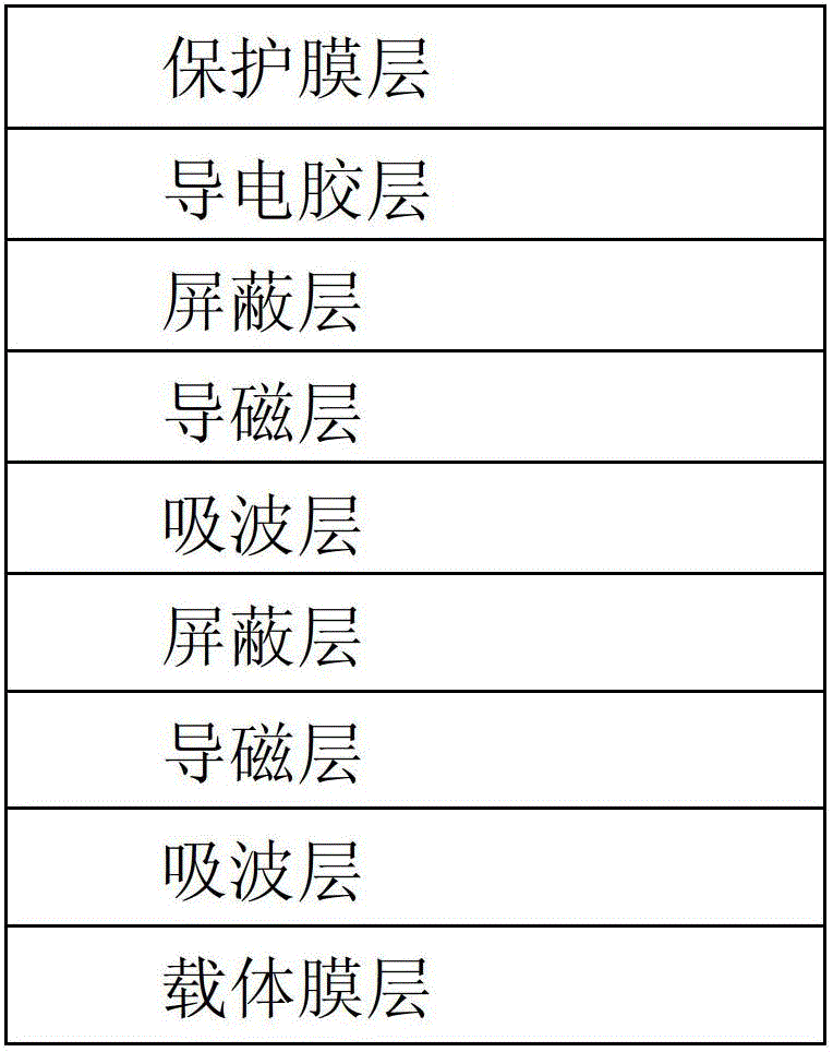
[0120] like figure 1 As shown, the wave-absorbing magnetic shielding film of the present invention includes a carrier film layer 1 , a wave-absorbing layer 2 , a magnetic-conducting layer 3 , a shielding layer 4 , a conductive adhesive layer 5 and a protective film layer 6 from inside to outside.

[0121] 1. Make the carrier film layer:

[0122] Except that the voltage in the corona pretreatment process is 10000V to make the surface tension reach 40 dynes, the drying temperature is 180°C, the resin content in the subsequent layer is 20%, and the thickness of the subsequent layer is 5 μm, the rest are the same as in the embodiment 1 is the same.

[0123] 2. Overlay absorbing layer:

[0124] On the surface of the adhesive layer, continue to apply the wave-absorbing coating by means of rubber rollers, with a coating thickness of 50 μm, and dry to form a wave-absorbing layer after coating. The drying time is 5 minutes, and the drying temperature is 200 ° C.

[0125] Wherein, th...


PUM

PropertyMeasurementUnit
Thicknessaaaaaaaaaa
Widthaaaaaaaaaa
Thicknessaaaaaaaaaa

Abstract

The invention discloses a wave-absorbing magnetic-conductive shielding film and a manufacture method thereof. The wave-absorbing magnetic-conductive shielding film has a layered structure. Through reasonable superposition of a wave-absorbing layer, a magnetic conductive layer and a shielding layer, the wave-absorbing magnetic-conductive shielding film has a quite good shielding effect for electromagnetic waves with a frequency of 100MHz to 10GHz, and the electromagnetic shielding efficiency can reach more than 80DB. The preparation method is carried out by use of a mode of combining routine coating and magnetron sputtering, the operation is simple, and a formed film layer is light, thin and compact. Therefore, the wave-absorbing magnetic-conductive shielding film and the manufacture method are applied to various electronic products and communication devices.

Description

technical field [0001] The invention belongs to the field of communication, in particular to a wave-absorbing magnetic shielding film and a manufacturing method thereof. Background technique [0002] Various electronic products and equipment in the communication field will form many electromagnetic waves to interfere with each other in space, which will not only cause damage to themselves and the environment, but also make it difficult to achieve high-frequency and high-speed transmission. Electromagnetic shielding film can limit the mutual propagation of electromagnetic waves between electronic product components and between electronic products and the environment, reduce the damage caused by electromagnetic interference, and is widely used in the field of communication. [0003] However, the traditional electromagnetic shielding film has the following two defects: first, in terms of raw materials, the selection of shielding materials can realize the shielding effect by ref...

Claims


Application Information

Patent Timeline
IPC IPC(8): H05K9/00C23C14/35
Inventor 祝琼
Owner 广州宏庆电子有限公司
Why Eureka
Try Eureka