Circuit board and electronic device

A technology for circuit substrates and capacitors, used in circuit substrate materials, electrical solid devices, printed circuit components, etc., can solve the problems of unstable operation, poor connection, and unbalance of inverter circuits, and eliminate poor connections and reduce The effect of impedance

Inactive Publication Date: 2014-09-10
SUMITOMO BAKELITE CO LTD
View PDF9 Cites 1 Cited by
  • Summary
  • Abstract
  • Description
  • Claims
  • Application Information

AI Technical Summary

Problems solved by technology

[0010] When the circuit board on which the switching element is mounted and the circuit board on which the driving circuit is mounted are different like the inverter circuit of Patent Document 2, it is difficult to shorten the lead wire between the switching element and the driving circuit.
Therefore, the impedance of the wiring between the switching element and the drive circuit increases, and the inverter circuit is easily affected by noise and current imbalance.
As a result, there is a problem that the operation of the inverter circuit becomes unstable
In addition, since it is necessary to realize the electrical connection between the switching element and the drive circuit through the connection terminal, the level of the signal decreases and the SN ratio changes due to poor connection and contact resistance of the connection part between the connection terminal and the drive circuit. Difference
There is a problem that the operation of the inverter circuit becomes unstable due to such a deterioration of the SN ratio

Method used


Image

  • Circuit board and electronic device
  • Circuit board and electronic device
  • Circuit board and electronic device

Examples


no. 1 Embodiment approach >

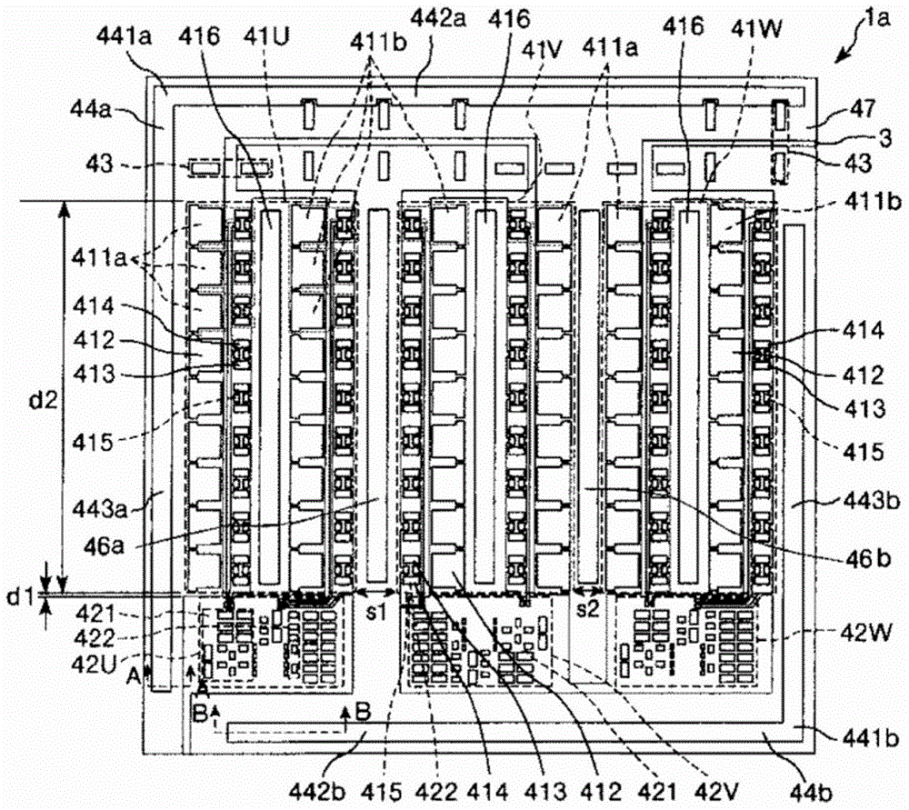
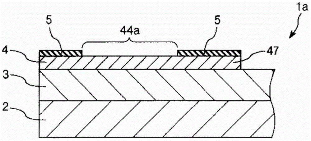
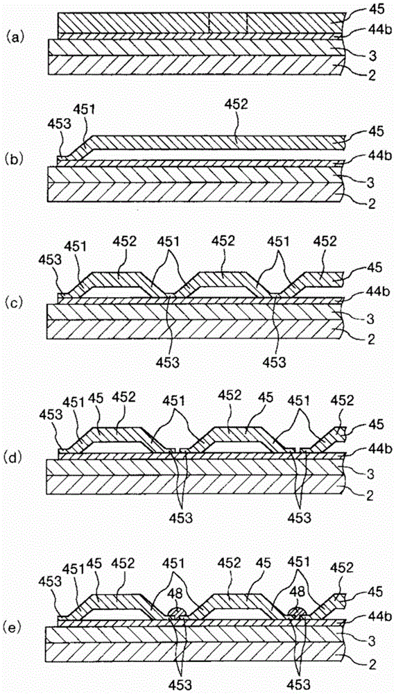
[0106] figure 1 It is a plan view showing the first embodiment of the circuit board of the present invention. figure 2 yes figure 1 A-A line sectional view of the circuit board shown. image 3 is expressed in figure 1 A diagram showing an example of the configuration of the additional conductor provided on the circuit board shown. Figure 4 yes image 3 Perspective view of the foot of the additional conductor shown. Figure 5 It is a plan view showing an embodiment of the electronic device of the present invention. Figure 6 yes Figure 5 Circuit diagram of the series circuit of the switching arms with the electronic device shown. where, in the description below, the figure 1 set the upper side to "Up", the lower side to "Bottom", the left side to "Left", the right side to "Right", and the figure 2 as well as image 3 The description will be made by referring to the upper side as "upper side" and the lower side as "lower side".

[0107] figure 1 The circuit board...

no. 2 Embodiment approach >

[0208] Next, based on Figure 7 A second embodiment of the present invention will be described.

[0209] Figure 7 It is a plan view showing the second embodiment of the circuit board of the present invention. Hereinafter, the second embodiment will be described focusing on the points of difference from the first embodiment described above, and descriptions of the same contents will be omitted.

[0210] That is, the circuit board 1b according to the second embodiment is the same as that of the first embodiment except for the arrangement of the second drive circuit terminal group 42V and the capacitor terminal 43. Composition, description omitted.

[0211] Such as Figure 7 As shown, like the circuit board 1a of the first embodiment, the second terminal group for switching arm series circuits 41V is disposed opposite to the first terminal group for switching arm series circuits 41U and the third terminal group for switching arm series circuits 41W. Flip 180 degrees.

[02...


PUM

PropertyMeasurementUnit
Thermal conductivityaaaaaaaaaa
Thicknessaaaaaaaaaa
Thicknessaaaaaaaaaa

Abstract

Provided are: a circuit board that can increase the operational stability of a mounted circuit; and an electronic device that uses the circuit board. The circuit board (1a) is provided with: a metal substrate (2); an insulating layer (3) provided to one surface of the metal substrate (2); and a conductor layer (4) provided on the insulating layer (3). The conductor layer (4) is provided with a wiring pattern having: switching arm series circuit terminal groups (41U, 41V, 41W) configured from a plurality of switching element terminals for connecting switching elements; and drive circuit terminal groups (42U, 42V, 42W) configured from a plurality of drive circuit terminals for connecting drive circuits that impose a driving voltage on the switching elements. The switching arm series circuit terminal groups (41U, 41V, 41W) and the drive circuit terminal groups (42U, 42V, 42W) are formed on the same surface.

Description

technical field [0001] The present invention relates to a circuit board for mounting a switching element and an electronic device having a switching element mounted on the circuit board. Background technique [0002] In recent years, along with the high performance and miniaturization of electronic equipment, there is a tendency to demand high density and high functionality of semiconductors. Under such a tendency, in a circuit composed of heat-generating elements such as switching elements, the operation of the circuit may become unstable due to heat generated by current flowing through the active elements and temperature rise. [0003] Examples of active elements that generate heat by driving include switching elements such as MOSFETs (MetalOxide Semiconductor Field Effect Transistors) and IGBTs (Insulated Gate Bipolar Transistors). Light emitting elements such as organic EL (Electro Luminescence, electroluminescence), LED (Light Emitting Diode, light emitting diode). ...

Claims


Application Information

Patent Timeline
IPC IPC(8): H01L25/07H01L23/36H01L25/18
CPCH01L23/36H01L2924/0002H05K1/0265H05K2201/10272H02M7/003H05K2201/10166H05K1/05H01L2924/00
Inventor 八木茂幸新居良英
Owner SUMITOMO BAKELITE CO LTD
Why Eureka
Try Eureka