
Pixel circuit and display device

A pixel circuit and display device technology, applied to static indicators, instruments, etc., can solve the problem of uneven display brightness of display devices, achieve the effects of reducing the number of signal lines, increasing pixel density, and reducing costs

Active Publication Date: 2016-08-31
BOE TECH GRP CO LTD +1
View PDF6 Cites 0 Cited by
  • Summary
  • Abstract
  • Description
  • Claims
  • Application Information

AI Technical Summary

Problems solved by technology

[0006] The purpose of the present invention is to solve the problem of uneven display brightness of a display device, reduce the number of signal lines used for pixel circuits in the display device, reduce the cost of integrated circuits, and increase pixel density at the same time

Method used


Image

  • Pixel circuit and display device
  • Pixel circuit and display device
  • Pixel circuit and display device

Examples


Embodiment Construction

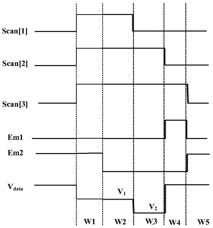
[0030] The specific implementation manners of the present invention will be further described below in conjunction with the drawings and examples. The following examples are only used to illustrate the technical solution of the present invention more clearly, but not to limit the protection scope of the present invention.

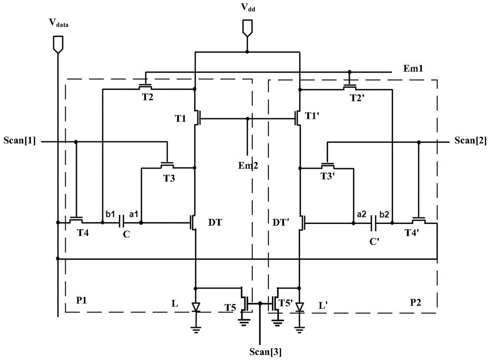
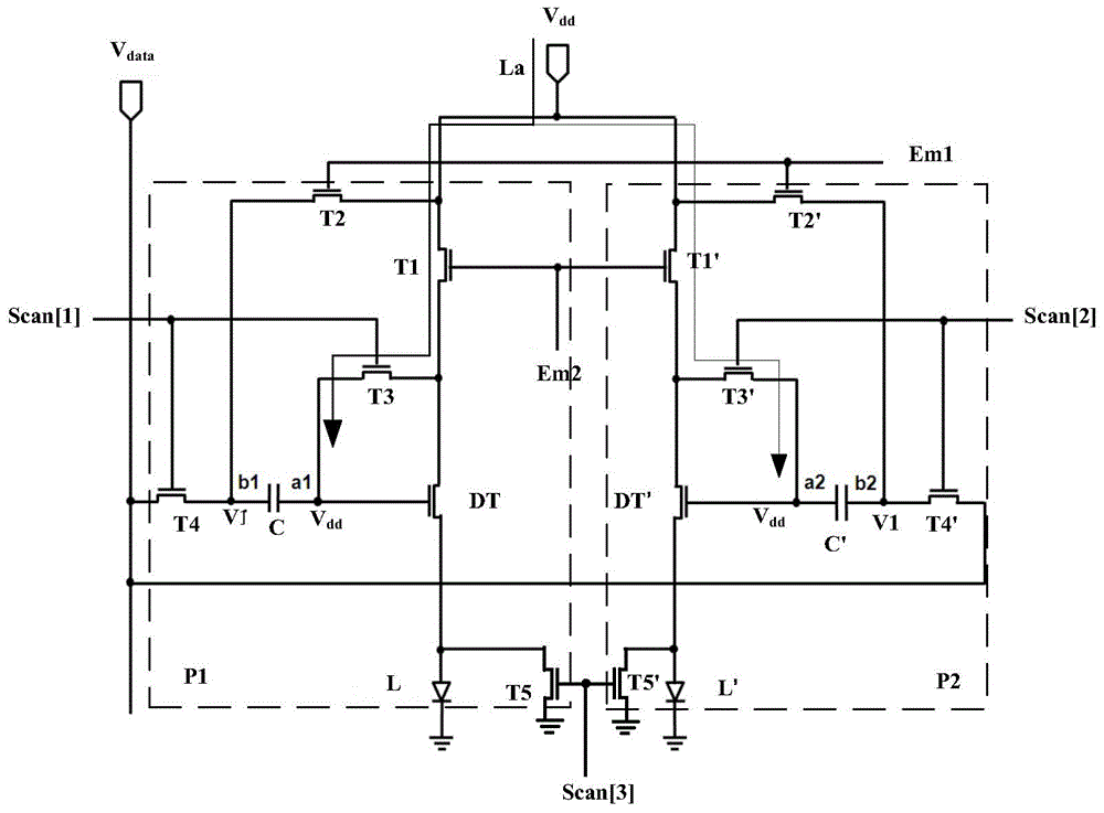
[0031] An embodiment of the present invention provides a pixel circuit, such as figure 1 Or as shown in Figure 3, it includes: two sub-pixel circuits P1 and P2 with the same structure, where each sub-pixel circuit corresponds to a pixel; since P1 and P2 have the same structure, the following only combines the structure of P1 for the two sub-pixel circuits Be explained;

[0032] P1 here includes: five switching units T1, T2, T3, T4, T5, a driving unit DT, an energy storage unit C, and an electroluminescence unit L (for the convenience of distinction, in figure 1 Or in Figure 3, the five switching units in P2 are represented as T1', T2', T3', T4', T5' respe...


PUM


Abstract

The present invention provides a pixel circuit and a display device, the pixel circuit includes two sub-pixel circuits, each sub-pixel circuit includes: each sub-pixel circuit includes: five switching units, a driving unit, an energy storage unit and an electroluminescence unit, The two sub-pixel circuits share the same data voltage line and a plurality of scanning signal lines. In the pixel circuit provided by the present invention, the operating current flowing through the electroluminescent unit device is not affected by the threshold voltage of the corresponding drive transistor, which completely solves the problem of uneven display brightness caused by the drift of the threshold voltage of the drive transistor. At the same time, in the present invention, a compensation circuit is used to complete the driving of two pixels, and two adjacent pixels share a plurality of signal lines, which can reduce the number of signal lines used in the pixel circuit in the display device, reduce the cost of the integrated circuit, and reduce the Pixel pitch to increase pixel density.

Description

technical field [0001] The present invention relates to the field of display technology, in particular to a pixel circuit and a display device. Background technique [0002] Organic light-emitting display (OLED) is one of the hot spots in the field of flat panel display research. Compared with liquid crystal display, OLED has the advantages of low energy consumption, low production cost, self-illumination, wide viewing angle and fast response speed. At present, OLEDs have begun to replace traditional liquid crystal (LCD) displays in display fields such as mobile phones, PDAs, and digital cameras. Pixel drive circuit design is the core technical content of OLED display, which has important research significance. [0003] Unlike TFT-LCD (Thin Film Field Effect Transistor Liquid Crystal Display) which uses a stable voltage to control brightness, OLED is current driven and requires a stable current to control light emission. [0004] Due to the process and device aging, in the...

Claims


Application Information

Patent Timeline
Patent Type & Authority Patents(China)
IPC IPC(8): G09G3/3233G09G3/3225
CPCG09G3/32G09G3/3233
Inventor 杨盛际
Owner BOE TECH GRP CO LTD
Features
  • Generate Ideas
  • Intellectual Property
  • Life Sciences
  • Materials
  • Tech Scout
  • Unparalleled Data Quality
  • Higher Quality Content
  • 60% Fewer Hallucinations
Learn More