Laser annealing device and method

A laser annealing and laser technology, applied in laser welding equipment, electrical components, circuits, etc., can solve the problems of dual-laser IGBT annealing and low laser utilization, and achieve the effect of improving absorption efficiency, ensuring activation efficiency, and improving utilization efficiency

Active Publication Date: 2014-10-01
SHANGHAI MICRO ELECTRONICS EQUIP (GRP) CO LTD
View PDF7 Cites 4 Cited by
  • Summary
  • Abstract
  • Description
  • Claims
  • Application Information

AI Technical Summary

Problems solved by technology

[0005] In the technical scheme disclosed in the document "Double Pulse Laser Annealing Technology and Application", although the control of laser energy and temperature is relatively flexible, since the reflectivity of vertical incidence i

Method used


Image

  • Laser annealing device and method
  • Laser annealing device and method
  • Laser annealing device and method

Examples


Embodiment Construction

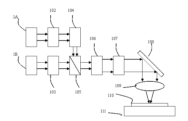
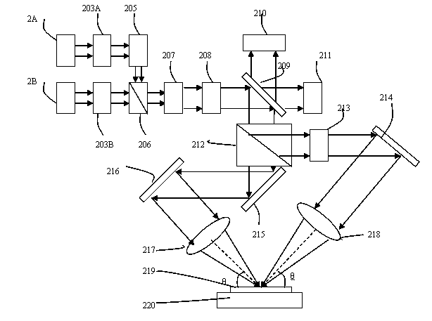
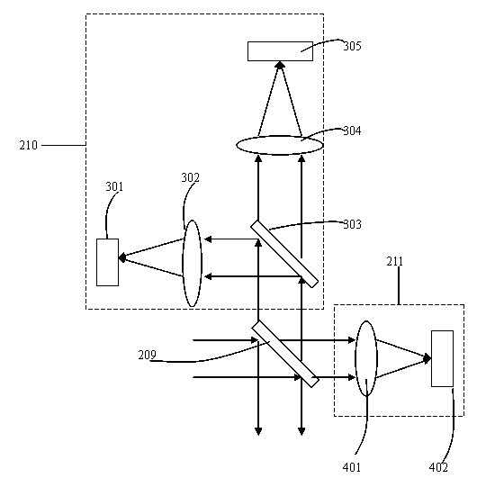
[0026] Specific embodiments of the present invention will be described in detail below in conjunction with the accompanying drawings.

[0027] For ease of understanding, some relevant definitions are explained below:

[0028] When light travels through the surface of an optical component, such as a beamsplitter, at non-perpendicular angles, both reflection and transmission properties depend on polarization phenomena. In this case, the coordinate system used is defined by the plane containing the input and reflected beams. If the polarization vector of the ray is in this plane, it is called P polarization; if the polarization vector is perpendicular to this plane, it is called S. polarization. Any input polarization state can be expressed as a vector sum of S and P components.

[0029] When natural light is reflected and refracted on the dielectric interface, the reflected light and refracted light are generally partially polarized light. Only when the incident angle is a cer...


PUM

PropertyMeasurementUnit
Wavelengthaaaaaaaaaa

Abstract

The invention discloses a laser annealing device and a method. The device comprises a laser source, a light path part, a light path monitoring part and a motion part, wherein the laser source comprises two P-pole linear polarization laser devices; and laser beams emitted by the two P-pole linear polarization laser devices pass through the light path part, are treated by a beam splitting part, and then are emitted to the surface of a silicon wafer of the motion part at near brewster angles. Compared with the prior art, the laser annealing device adopts the two P-pole linear polarization laser devices, light emitted from a laser device is converted into S-pole polarized light, the S-pole polarized light is synthesized and then passes through a light path treatment part, then two light beams are separated, the S-pole light beam is reduced to P-pole light, and finally the two light beams are emitted at brewster angles. Therefore, the two laser beams can be emitted at the brewster angles, the light path treatment part is not too complicated, and the utilization efficiency of laser energy is improved greatly.

Description

technical field [0001] The invention relates to the field of integrated circuit equipment manufacturing, in particular to a laser annealing device and method. Background technique [0002] In the semiconductor manufacturing process, in order to adjust the conductivity of the local area on the surface of the silicon wafer, ion implantation technology is widely used to do impurity doping on a specific area on the surface of the silicon wafer. After ion implantation, since the doped impurity atoms are in the state of defects in the silicon lattice, annealing treatment is generally required. On the one hand, it can eliminate the damage caused by the doping to the semiconductor material lattice, and on the other hand, it can effectively activate the doped impurities. . [0003] At present, laser annealing generally adopts laser annealing for ion activation. A general laser annealing device mainly includes: a laser source, an optical path part, an optical path monitoring part a...

Claims


Application Information

Patent Timeline
IPC IPC(8): H01L21/268B23K26/067
CPCB23K26/0643B23K26/0652B23K26/067H01L21/268
Inventor 刘国淦兰艳平
Owner SHANGHAI MICRO ELECTRONICS EQUIP (GRP) CO LTD
Why Eureka
Try Eureka