Anti-fuse structure and method for forming the same

A technology of anti-fuse and isolation structure, which is applied in the direction of electrical components, electric solid-state devices, circuits, etc., can solve the problems of high programming voltage and difficulty in making high-voltage transistors, and achieve the effect of increasing process costs

Active Publication Date: 2014-10-15
SEMICON MFG INT (SHANGHAI) CORP
View PDF4 Cites 4 Cited by
  • Summary
  • Abstract
  • Description
  • Claims
  • Application Information

AI Technical Summary

Problems solved by technology

However, due to the fact that the thickness of the gate oxide layer is still relatively large, the programming voltage for programming the gate oxide layer antifuse is relatively large, and a high-voltage transistor is required to generate the programming voltage.
With the continuous decline of semiconductor process nodes, the production of high-voltage transistors will become more and more difficult

Method used


Image

  • Anti-fuse structure and method for forming the same
  • Anti-fuse structure and method for forming the same
  • Anti-fuse structure and method for forming the same

Examples


Embodiment Construction

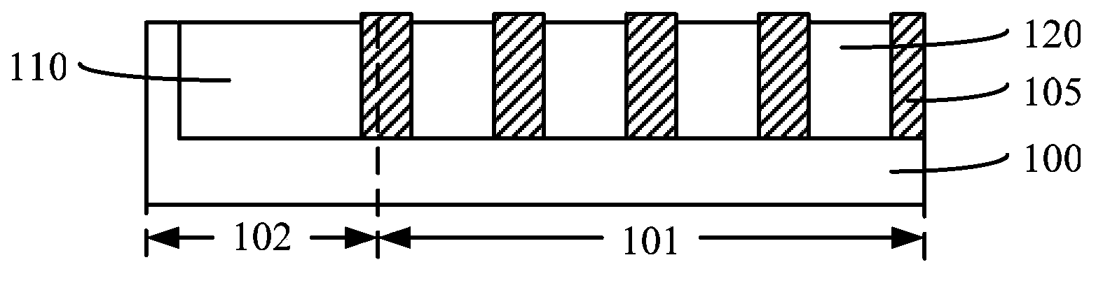
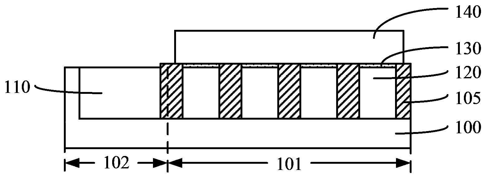
[0026] In the process of forming MOS transistors using the existing CMOS process, because the thickness of the formed gate oxide layer is too low, it is easy to cause breakdown or leakage. Therefore, the thickness of the gate oxide layer corresponding to each process node is limited. will be reduced without limit. For the gate oxide antifuse, since the gate oxide layer needs to be broken down to activate the antifuse, a thicker gate oxide layer will result in a higher programming voltage for programming the gate oxide layer antifuse, which requires the use of A high voltage transistor generates the programming voltage. With the continuous decline of semiconductor process nodes, the manufacture of high-voltage transistors will become more and more difficult.

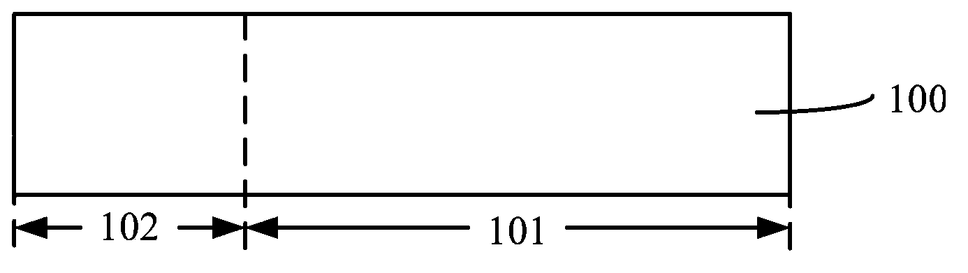
[0027] To this end, the inventors have proposed an antifuse structure and a method for forming the same. A gate oxide layer is formed on the entire surface of the active region surrounded by the shallow trench isolation ...


PUM


Abstract

An anti-fuse structure and a method for forming the same. The anti-fuse structure includes: a semiconductor substrate including an anti-fuse area and an interconnection area; a shallow trench isolation structure located inside the semiconductor substrate and isolating the anti-fuse area into at least one active area; a gate oxide located on an entire surface of the active area, the thickness of a gate oxide on an edge position of the active area is smaller than that of a gate oxide in a middle position; a gate electrode located on a surface of the gate oxide and a surface of part of the shallow trench isolation structure; and a first electrode located on a surface of the interconnection area of the semiconductor substrate, the first electrode being electrically connected with the active area. Since a thinner gate oxide is formed on an edge part of the whole active area, the area of the thinner gate oxide becomes larger, and thus a programming voltage for programming of gate oxide anti-fuse is reduced.

Description

technical field [0001] The invention relates to semiconductor technology, in particular to an antifuse structure and a forming method thereof. Background technique [0002] Fuses and antifuses are widely used in today's integrated circuits to selectively connect or disconnect a device from the rest of the circuit, as well as to provide logic operations. A fuse interrupts or breaks an electrical connection by activating (melting, opening, etc.) the fuse, increasing circuit resistance to provide a logical difference between activated and deactivated fuse devices. The anti-fuse and the fuse work in the opposite way. The anti-fuse is non-conductive when it is not activated, and becomes a conductor after activation (breakdown, metal diffusion, amorphous silicon to polysilicon, etc.), forming an electrical current. A connection can selectively allow two devices or chips that are otherwise electrically isolated to be electrically connected, and can provide different resistance val...

Claims


Application Information

Patent Timeline
Patent Type & Authority Applications(China)
IPC IPC(8): H01L23/525H01L29/417H01L21/768H01L21/283
Inventor 冯军宏甘正浩
Owner SEMICON MFG INT (SHANGHAI) CORP
Why Eureka
Try Eureka