Vertical laminated optical path module and multi-die semiconductor laser

A technology of semiconductors and lasers, applied in the field of lasers, can solve problems such as difficult mass production of multi-die semiconductor lasers, inability to guarantee product process repeatability, poor disassembly, etc. Effect of space utilization and cost reduction

Inactive Publication Date: 2014-10-22
BWT BEIJING
View PDF6 Cites 8 Cited by
  • Summary
  • Abstract
  • Description
  • Claims
  • Application Information

AI Technical Summary

Problems solved by technology

Since the CoS is welded on the bottom plate, if one fails, it needs to be replaced again, and the bottom plate is made of metal with high thermal conductivity. During the process of replacing the CoS, other unit devices will be affected, and they need to be adjusted again. However, this space integration method

Method used


Image

  • Vertical laminated optical path module and multi-die semiconductor laser
  • Vertical laminated optical path module and multi-die semiconductor laser
  • Vertical laminated optical path module and multi-die semiconductor laser

Examples


Embodiment Construction

[0056] In order to make the object, technical solution and advantages of the present invention clearer, the implementation manner of the present invention will be further described in detail below in conjunction with the accompanying drawings.

[0057] The invention modularizes the unit devices in the semiconductor laser, and vertically distributes multiple optical paths on the heat sink module in order to fully utilize the space utilization rate to form a vertical stacked optical path module.

[0058] Example 1 of vertically stacked optical path module

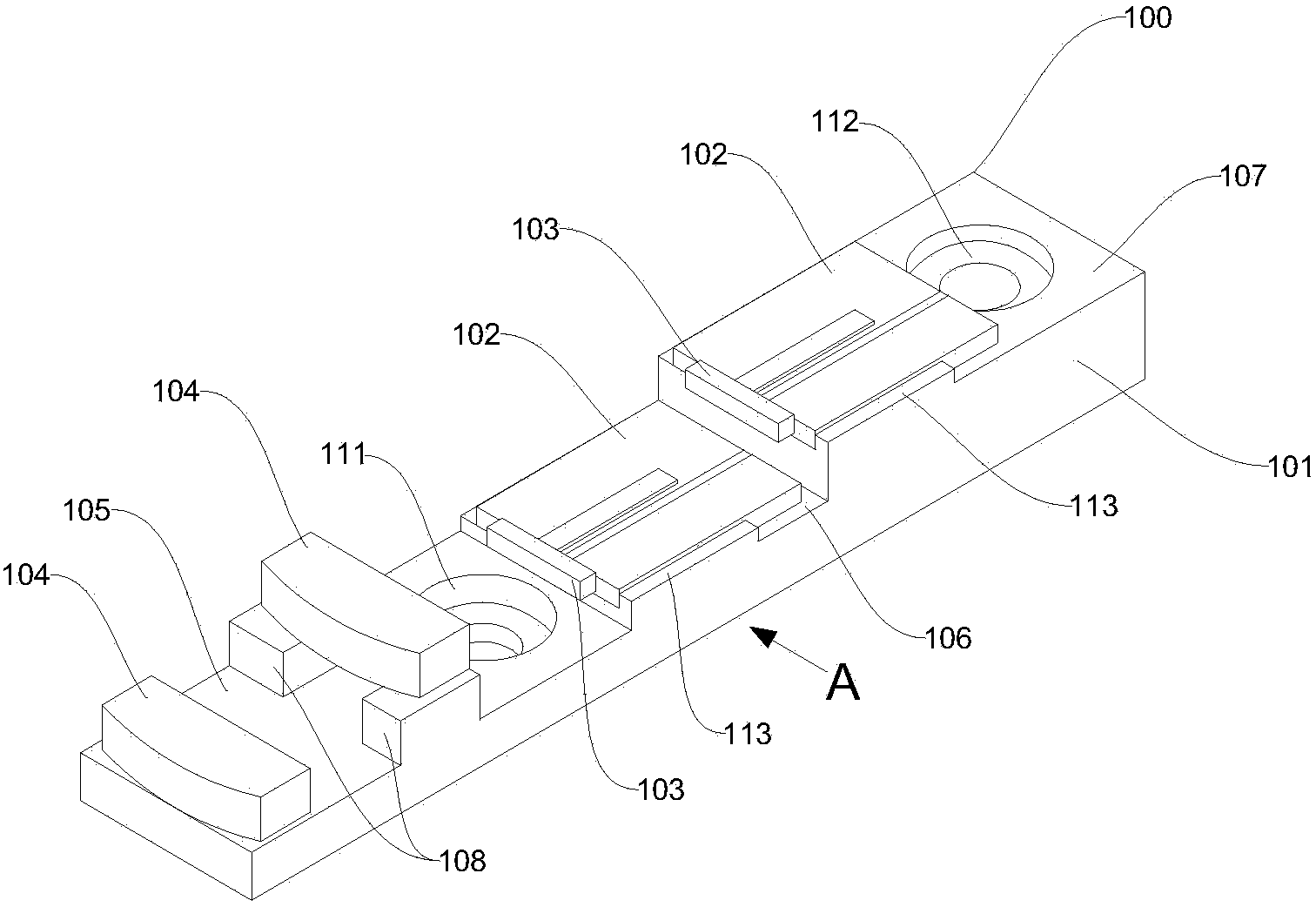
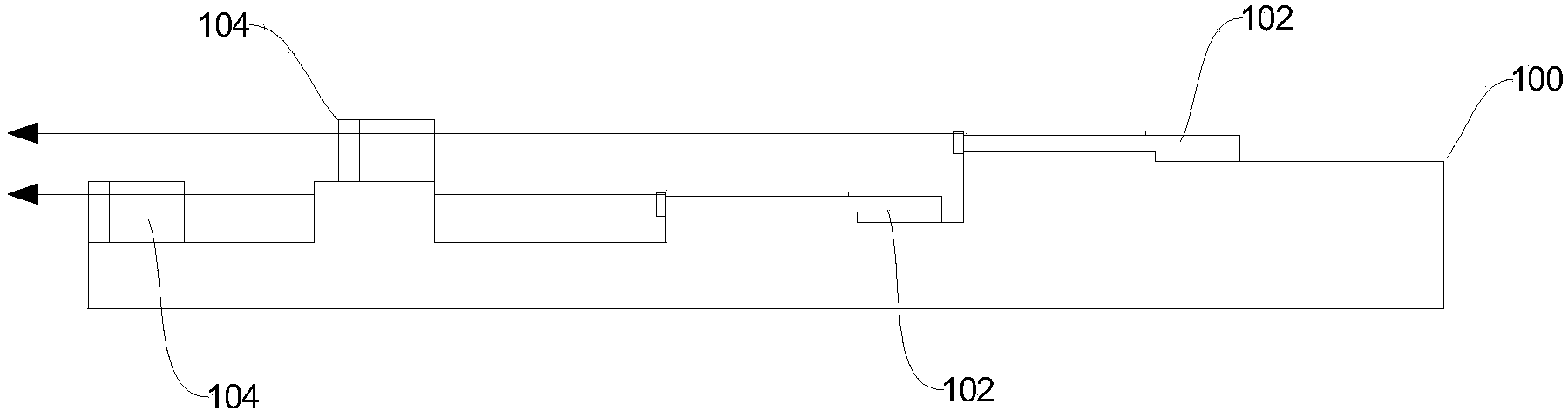
[0059] figure 1 It is a structural schematic diagram of Embodiment 1 of the vertical stacked optical path module in the present invention; figure 2 It is an A-direction view of Embodiment 1 of the vertically stacked optical path module in the present invention. Such as figure 1 and figure 2 As shown, the present invention discloses a vertical stacked optical path module 100, including: a heat sink module 101 and two opt...


PUM


Abstract

The invention relates to the technical field of laser, and particularly relates to a vertical laminated optical path module and a multi-die semiconductor laser. The vertical laminated optical path module comprises a heat sink module and N optical path units, N being a positive integer larger than or equal to 2. Each optical path unit comprises a semiconductor laser chip CoS with auxiliary heat sink, a fast axis collimating lens and a slow axis collimating lens. One surface of the heat sink module is in the shape N+1 steps, from the first step to the N+1 steps from low to high, wherein the first step is provided with N-1 lens frames. The multi-die semiconductor laser comprises a step-shaped bottom board and a plurality of vertical laminated optical path modules, wherein the plurality of vertical laminated optical path modules are fixed to the different steps of the step-shaped bottom board respectively. According to the vertical laminated optical path module and the multi-die semiconductor laser, modularization of a plurality of optical paths are realized, process repeatability and stability are guaranteed, and space utilization rate of the multi-die semiconductor laser is improved.

Description

technical field [0001] The invention relates to the field of laser technology, in particular to a vertical stacked optical path module and a multi-tube-core semiconductor laser. Background technique [0002] In current multi-die semiconductor lasers, optical components such as multiple semiconductor laser chips (CoS) with auxiliary heat sinks, multiple fast-axis collimating lenses, and multiple slow-axis collimating lenses are usually integrated on the same base plate. , and in order to increase the power of the semiconductor laser, more unit devices are usually integrated, so that the space occupied by the entire semiconductor laser in the horizontal direction will increase significantly; when working, the beam emitted by each CoS passes through the slow axis of the fast axis collimator lens After being collimated by the collimating lens, it becomes a parallel beam, which is then turned by the reflector, reflected to the coupling mirror for convergence, and finally coupled ...

Claims


Application Information

Patent Timeline
IPC IPC(8): H01S5/022H01S5/024
Inventor 杨朝栋姜笑尘刘瑞高燕燕何晓光
Owner BWT BEIJING
Why Eureka
Try Eureka