Organic light-emitting device, manufacturing method and display panel

A technology of organic light-emitting devices and manufacturing methods, which is applied in the fields of organic semiconductor devices, semiconductor/solid-state device manufacturing, and electric solid-state devices. and other issues to achieve high resolution and improve yield

Inactive Publication Date: 2014-11-12
EVERDISPLAY OPTRONICS (SHANGHAI) CO LTD
View PDF4 Cites 16 Cited by
  • Summary
  • Abstract
  • Description
  • Claims
  • Application Information

AI Technical Summary

Problems solved by technology

[0005] The emission spectrum of WOLED covers the region from blue light to red light. When applied in the micro-resonator structure of top-emitting organic light-emitting devices, the light may interfere constructively or destructively in different color regions; WOLED generally uses full The mask of the opening is made, so the film thickness of the three positions of the three primary colors RGB is the same, and the micro-resonant cavity cannot be adjusted by adjusting the film thickness, so that constructive interference of all luminous wavelengths (RGB) cannot be achieved
[0006] In summary, the existing WOLEDs cannot be applied to top-emitting organic light-emitting devices because they cannot overcome the problem of micro-resonator adjustment.

Method used


Image

  • Organic light-emitting device, manufacturing method and display panel
  • Organic light-emitting device, manufacturing method and display panel
  • Organic light-emitting device, manufacturing method and display panel

Examples


Embodiment Construction

[0035] The present invention will be further described below with reference to the accompanying drawings and specific embodiments, but it is not intended to limit the present invention.

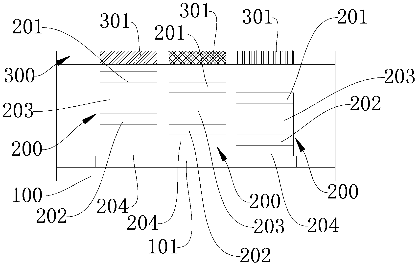
[0036] The technical solution of the present invention includes an organic light-emitting device, such as figure 1 As shown, there are a plurality of light-emitting units 200 formed on a substrate 100 and isolated from each other, each light-emitting unit 200 includes a semi-reflective cathode 201, a transparent anode 202 and sandwiched between the semi-reflective cathode 201 and the transparent anode 202 the WOLED layer 203;

[0037] The substrate 100 is provided with a reflective anode 101 shared by a plurality of light-emitting units 200 to reflect light upward, and a respective light-emitting unit 200 is provided between the transparent anode 202 of each light-emitting unit 200 and the common reflective anode 101 . an independent optical adjustment layer 204 for adjusting the wavelength ...


PUM


Abstract

An organic light emitting device relates to a WOLED based Top emission organic light emitting device and the manufacturing method thereof and a display panel which applies the organic emitting device. In the organic light emitting device, a plurality of emitting units are formed on a substrate and isolated respectively; a plurality of independent optical adjustment layers are formed between the reflective electrode and the transparent positive electrode of each emitting unit respectively; a color filter layer is formed above the emitting units. This embodiment applies the structure of WOLED into the top emission device, the mask having a maximum aperture ratio in the evaporation process, consequently, it improved yield rate of display panel manufacturing, reduced the costing of the evaporation process and improved the resolution of the display panel.

Description

technical field [0001] The invention relates to an organic light-emitting device, in particular to a top-emission type organic light-emitting device based on WOLED (White Organic Light Emitting Diode), a manufacturing method thereof, and a display panel formed by using the organic light-emitting device. . Background technique [0002] At present, the high-pixel flat display panel is the market trend, and the AMOLED (Active Matrix / Organic Light Emitting Diode, active matrix organic light-emitting diode panel) panel has attracted everyone's attention. [0003] AMOLED panels occupy a dominant position in the small and medium-sized panel market with a pixel of 200ppi, and AMOLED WVGA (Wide Video Graphics Array, a resolution higher than VGA resolution: 800*480; ~200ppi) is the current mainstream resolution , and high pixel 250ppi, 300ppi and 350ppi will be the future development trend. The existing AMOLED panel production method is mainly based on Side by Side (side by side) te...

Claims


Application Information

Patent Timeline
Patent Type & Authority Applications(China)
IPC IPC(8): H01L27/32H01L51/52H01L51/56
CPCH01L51/5271H01L27/3244H01L51/5218H01L51/56H01L51/5234H10K59/35H10K59/38H10K50/852H10K50/125H10K50/856H10K59/12H10K59/1201H10K2102/351
Inventor 林信志
Owner EVERDISPLAY OPTRONICS (SHANGHAI) CO LTD
Why Eureka
Try Eureka