

A kind of high-density interconnection integrated circuit board manufacturing method
An integrated circuit board, high-density interconnection technology, applied in the directions of printed circuit manufacturing, printed circuit, printed circuit secondary processing, etc., can solve the problems of many production process links, insufficient safety and reliability, and low production efficiency, etc. Achieve the effect of improving production efficiency and production quality, improving reliability and safety, and enhancing electroplating uniformity
- Summary
- Abstract
- Description
- Claims
- Application Information
AI Technical Summary
Problems solved by technology
Method used
Image

Examples
Embodiment Construction
[0018] Further describe the technical scheme of the present invention in detail below in conjunction with accompanying drawing:
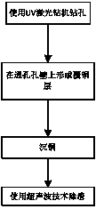
[0019] Such as figure 1 Shown, a kind of high-density interconnection integrated circuit board fabrication method, it comprises the following steps:
[0020] S1: Use a UV laser drill to drill through holes in the product area on the circuit board according to the design requirements, and drill test holes in the edge area of the board outside the product area;
[0021] S2: Use ordinary electroplating and micro-hole electroplating technology to form a copper clad layer on the plate surface, the wall of the via hole and the wall of the test hole, and fill the via hole and the test hole with resin after copper cladding;
[0022] S3: Carry out sinking copper treatment to plate;
[0023] S4: Use ultrasonic technology to remove slag from the board.
[0024] The stated test hole diameter is the same as the smallest via hole diameter in the product area...
PUM
 Abstract
Description
Claims
Application Information