Magnetron sputtering equipment and method

A magnetron sputtering and equipment technology, applied in the field of magnetron sputtering equipment, can solve problems such as low production input cost, and achieve the effects of reducing production input cost, increasing bonding force, reducing operating cost and technical risk

Active Publication Date: 2014-11-26
BEIJING NAURA MICROELECTRONICS EQUIP CO LTD
View PDF1 Cites 8 Cited by
  • Summary
  • Abstract
  • Description
  • Claims
  • Application Information

AI Technical Summary

Problems solved by technology

[0006] The present invention aims to solve the technical problems existing in the prior art, and provides a magnetron sputtering device and method, which can avoid the problem of metal electrode layer peeling, thereby improving product quality; in addition, it not only saves production input costs Lower, and can keep the original process basically unchanged, thus reducing operating costs and technical risks

Method used


Image

  • Magnetron sputtering equipment and method
  • Magnetron sputtering equipment and method
  • Magnetron sputtering equipment and method

Examples


Embodiment Construction

[0034]In order to enable those skilled in the art to better understand the technical solution of the present invention, the magnetron sputtering equipment and method provided by the present invention will be described in detail below with reference to the accompanying drawings.

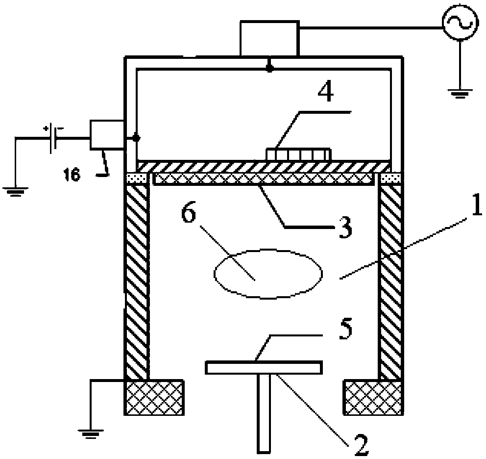
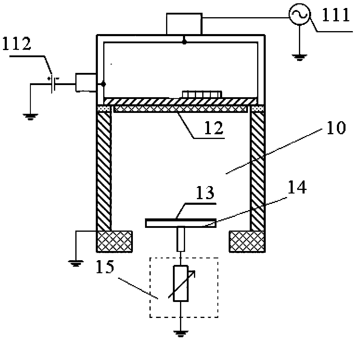
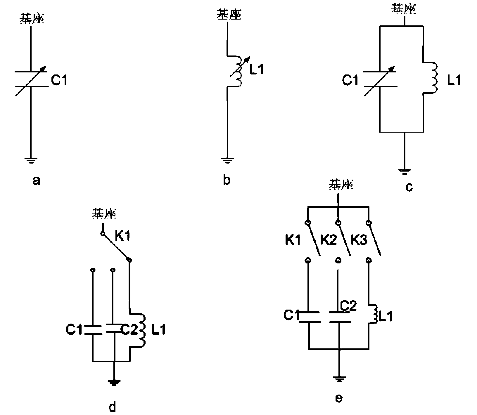
[0035] figure 2 It is a simplified structure diagram of the magnetron sputtering equipment provided by the first embodiment of the present invention. image 3 for figure 2 Circuit diagrams of five configurations of the medium bias cell. Please also refer to figure 2 and image 3 , the magnetron sputtering device includes a reaction chamber 10, a sputtering power supply, a bias unit 15 and a bombardment gas source (not shown in the figure). Wherein, a base 14 for carrying the workpiece 13 to be processed is arranged in the reaction chamber 10, and a target 12 is arranged at a position corresponding to the base 14 at the top of the reaction chamber 10; the sputtering power supply It is electrica...


PUM


Abstract

The invention provides magnetron sputtering equipment and method. The equipment and method are used for bombarding a thin film layer surface deposited on a machined workpiece surface after magnetron sputtering deposition, and therefore the thin film layer surface is made to be roughened. The magnetron sputtering equipment comprises a reaction cavity, a sputtering power source, a base, a target material, a bombardment gas source and a bias voltage unit, the sputtering power source is electrically connected with the target material, and is used for outputting sputtering power to the target material, and after magnetron sputtering deposition is completed, the bombardment gas source is used for leading bombardment gas which does not react with a thin film deposited on the machined workpiece surface into the reaction cavity, and the bombardment gas is excited by the bias voltage unit and/or the sputtering power source to form plasmas. The bias voltage unit is used for loading back bias voltages to the base so as to enable the plasmas to bombard the thin film surface, formed after magnetron sputtering deposition, of a machined workpiece. The magnetron sputtering equipment can solve the metal electrode layer peeling problem, the production investment cost is low, and the original technological process can be kept basically unchangeable.

Description

technical field [0001] The invention belongs to the technical field of microelectronic processing, and in particular relates to a magnetron sputtering device and method. Background technique [0002] In the process of preparing solar cells, LED chips, etc., magnetron sputtering equipment is usually used to deposit thin films (such as ITO, AZO) on the surface of the substrate. [0003] figure 1 It is a schematic structural diagram of a magnetron sputtering device. see figure 1 , the magnetron sputtering equipment includes a reaction chamber 1 , a chuck 2 , a target 3 and a magnetron 4 . Wherein, the chuck 2 is located at the bottom of the reaction chamber 1 for carrying the substrate 5; the target 3 is arranged on the top of the reaction chamber 1, and is connected to a power supply (not shown in the figure) arranged outside the reaction chamber 1 connected, the power supply provides a bias voltage to the target 3; the magnetron 4 is arranged above the target 3, and is dr...

Claims


Application Information

Patent Timeline
Patent Type & Authority Applications(China)
IPC IPC(8): C23C14/35
Inventor 陈鹏耿波
Owner BEIJING NAURA MICROELECTRONICS EQUIP CO LTD
Why Eureka
Try Eureka