Light alignment film and preparing method thereof, liquid crystal display substrate and device

A liquid crystal display and photo-alignment technology, applied in liquid crystal materials, chemical instruments and methods, optics, etc., can solve the problems of low contrast of liquid crystal display devices, residual decomposition products, and inability to guarantee

Inactive Publication Date: 2014-11-26
BOE TECH GRP CO LTD +1
View PDF6 Cites 17 Cited by
  • Summary
  • Abstract
  • Description
  • Claims
  • Application Information

AI Technical Summary

Problems solved by technology

[0004] However, there are at least the following problems in the above process technology: after the main curing of the alignment film, part of the reaction by-products (especially by-products with larger molecular weights) cannot be removed by heating, volatilization or transformation, that is, after heating, the by-products still remain Decomposition products may remain; moreover, even if the reaction product changes, there is no guarantee that the final reaction product will not have any effect on the orientation of the liquid crystal molecules
Therefore, impurities that affect the orientation of liquid crystal molecules may still remain in the existing photo-alignment film, resulting in defects such as low contrast, light leakage, and afterimages in the liquid crystal display device.

Method used


Image

  • Light alignment film and preparing method thereof, liquid crystal display substrate and device
  • Light alignment film and preparing method thereof, liquid crystal display substrate and device
  • Light alignment film and preparing method thereof, liquid crystal display substrate and device

Examples


preparation example Construction

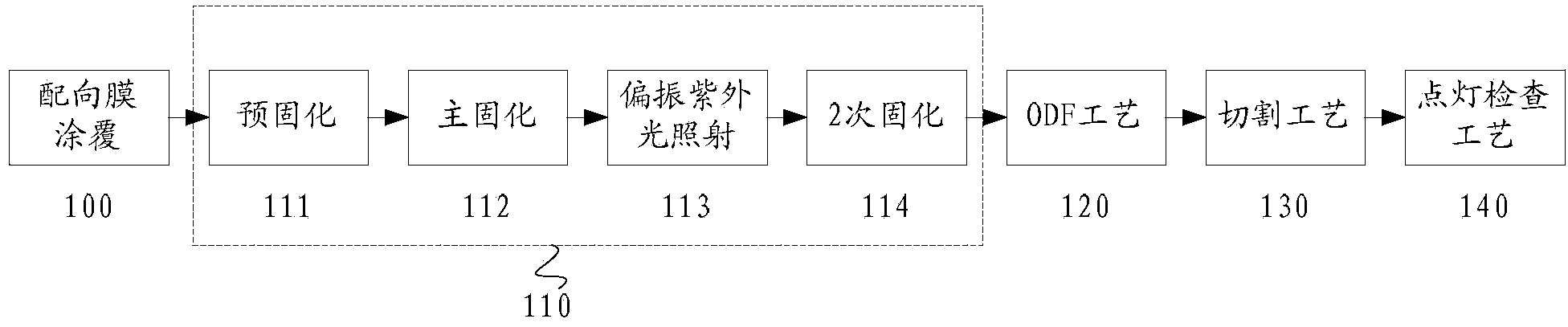
[0046] figure 2 A process flow diagram of a method for preparing a photo-alignment film provided in an embodiment of the present invention. Such as figure 2 As shown, the embodiment of the present invention provides a method for preparing a photo-alignment film, including:

[0047] Coating a photo-alignment material film layer on the substrate;

[0048] In this step, firstly, a layer of photo-alignment material film is coated on the substrate to prepare for preparing a photo-alignment film with an alignment function.

[0049] pre-curing the coated photo-alignment material film layer;

[0050] In this step, the coated photo-alignment material film layer is pre-cured. The purpose of the pre-cure is to make part of the photo-alignment material react and be better fixed on the substrate. Optionally, the temperature of the pre-curing step is 50-120° C., and the time is 0.5-10 minutes. Further preferably, the temperature of the pre-curing step is 60-100° C., and the time is 3...

Embodiment 1

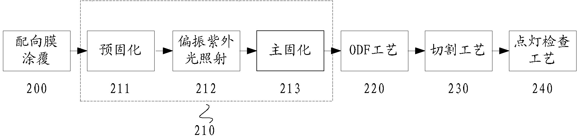
[0081] Such as figure 2 As shown, the photo-alignment material film layer 200 is coated on the substrate; the coated film layer is pre-cured at 50°C for 30 minutes—211°C; Irradiate at 254 nm to react part of the photo-alignment material to obtain the substrate 212 with the alignment function of the film layer of the photo-alignment material; main cure the substrate after the above steps at 180°C for 1 hour, and then cure the photo-alignment material film At the same time, the by-product 213 formed by the reaction is removed; after that, the ODF process 220, the cutting process 230, and the lighting inspection process 240 are sequentially performed to prepare the optical alignment film 1.

Embodiment 2

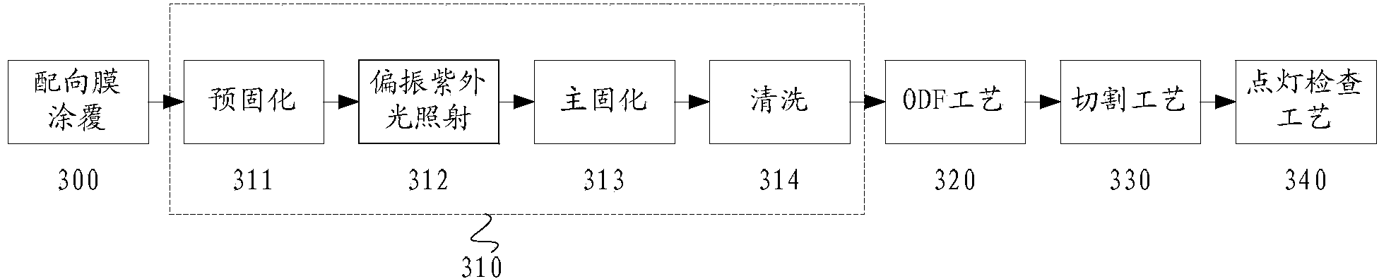
[0083] Such as image 3 As shown, the photo-alignment material film layer 300 is coated on the substrate; the coated film layer is pre-cured at 100° C. for 10 minutes—311; the pre-cured photo-alignment material film layer is linearly polarized Irradiate at 313nm to react part of the photo-alignment material to obtain the substrate 312 with the alignment function of the photo-alignment material film layer; main cure the substrate after the above steps at 300°C for 30 minutes, and then cure the photo-alignment material film At the same time, remove the by-products 313 formed by the reaction; perform a cleaning process 314 on the above-mentioned substrate; then perform an ODF process 320, a cutting process 330, and a lighting inspection process 340 in order to prepare a photoalignment film 2.


PUM


Abstract

The embodiment of the invention provides a light alignment film and a preparing method thereof, a liquid crystal display substrate and a device and belongs to the field of liquid crystal display. The light alignment film and the preparing method thereof, the liquid crystal display substrate and the device aim at improving the display effect of a display device. The preparing method of the light alignment film comprises the steps that the substrate is coated with a light alignment material film layer; the light alignment material film layer for coating is procured; the procured light alignment material film layer is irradiated with linearly polarized light, and thus the light alignment material film layer with the alignment function is formed; main curing is conducted on the light alignment material film layer with the alignment function, reaction by-products generated through the curing reaction are eliminated while the light alignment material film layer with the alignment function has the curing reaction, and the light alignment film is obtained. The light alignment film and the preparing method thereof, the liquid crystal display substrate and the device can be used in the production of the light alignment film.

Description

technical field [0001] The invention relates to the field of liquid crystal display, in particular to an optical alignment film and a preparation method thereof, a liquid crystal display substrate and a device. Background technique [0002] Thin Film Transistor Liquid Crystal Display (TFT-LCD) technology has become the mainstream technology of liquid crystal display at present. In the production of TFT-LCD, the alignment technology of liquid crystal molecules is very important. At present, the most widely used alignment technology in the production of TFT LCD is rubbing alignment (Rubbing alignment), which can provide strong alignment ability of liquid crystal molecules, but in the process of rubbing, rubbing with rubbing cloth often produces friction. Static electricity and particle pollution will not only cause damage to liquid crystal elements, but also cause various image quality problems such as MURA. [0003] In order to improve the picture quality and yield rate of ...

Claims


Application Information

Patent Timeline
Patent Type & Authority Applications(China)
IPC IPC(8): G02F1/1337C09K19/56
Inventor 杨发禄
Owner BOE TECH GRP CO LTD
Why Eureka
Try Eureka