Width measurement method
A measurement and width technology, applied in semiconductor/solid-state device testing/measurement, electrical components, circuits, etc., can solve problems such as unrecorded EBR/WEE width technical characteristics, achieve high repeatability, reduce errors, and simple principle Effect
- Summary
- Abstract
- Description
- Claims
- Application Information
AI Technical Summary
Problems solved by technology
Method used
Image
Examples
Embodiment Construction
[0022] The present invention will be further described below in conjunction with the accompanying drawings and specific embodiments, but not as a limitation of the present invention.
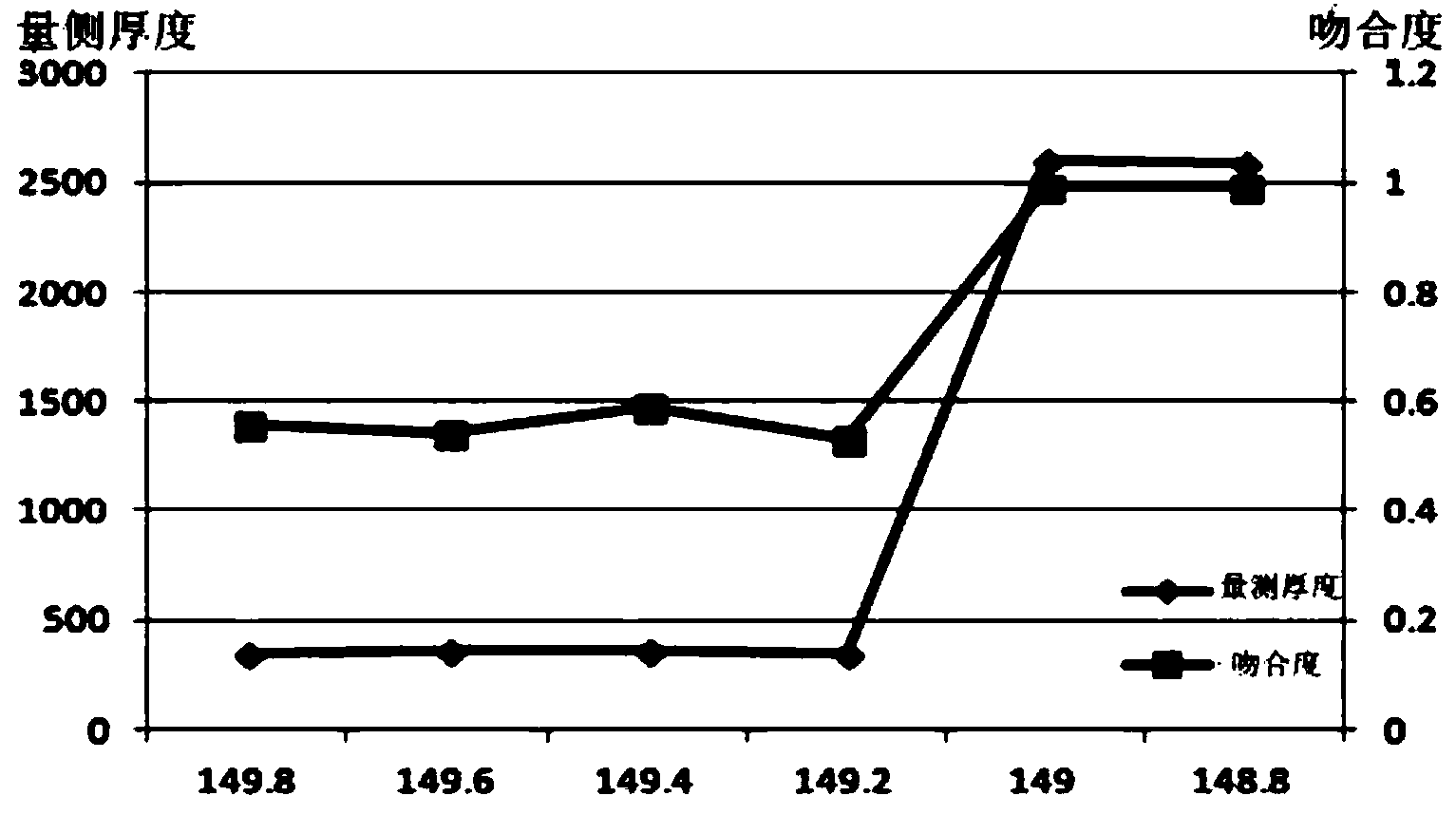
[0023] The present invention provides a method for measuring the width, and the method is used for photoresist thickness measurement because the width of EBR and WEE is a key process parameter in the semiconductor lithography process, and WEE (wafer edge exposure) is the In one step, use exposure light to expose the excess PR (positive photoresist) on the edge, and then develop the PR on the edge. After the positive photoresist is exposed, acidic substances will be produced, which will be removed by reaction with an alkaline developer. The length is about 2MM. And EBR (edge bead removal) is at the coater (coater), when the PR is applied, it is washed off with the nozzle (nozzle). The advantage of edge washing is that in general, the thickness of the PR on the edge of the wafer will be thicker. ...
PUM
 Abstract
Description
Claims
Application Information
 - R&D Engineer
- R&D Manager
- IP Professional
- Industry Leading Data Capabilities
- Powerful AI technology
- Patent DNA Extraction
Browse by: Latest US Patents, China's latest patents, Technical Efficacy Thesaurus, Application Domain, Technology Topic, Popular Technical Reports.
© 2024 PatSnap. All rights reserved.Legal|Privacy policy|Modern Slavery Act Transparency Statement|Sitemap|About US| Contact US: help@patsnap.com


