MEMS gas sensor and manufacturing method thereof

A technology of gas sensor and manufacturing method, which is applied in the direction of electric solid-state devices, semiconductor devices, instruments, etc., can solve the problems of affecting the heat insulation effect, deformation and rupture of devices, and rapid heat loss, etc., so as to solve heat loss, improve shock resistance and stability performance, enhance the effect of heat insulation

Active Publication Date: 2014-12-03
SUZHOU LEANSTAR ELECTRONICS TECH
View PDF7 Cites 36 Cited by
  • Summary
  • Abstract
  • Description
  • Claims
  • Application Information

AI Technical Summary

Problems solved by technology

[0006] (1) The stability is poor, and the device is deformed and cracked due to uneven force, resulting in device failure;
[0007] (2) The heat insulation effect is poor, and the air gap between the heat insulation tanks is large, resulting in faster heat loss, which affects the heat insulation effect

Method used


Image

  • MEMS gas sensor and manufacturing method thereof
  • MEMS gas sensor and manufacturing method thereof
  • MEMS gas sensor and manufacturing method thereof

Examples


Embodiment 1

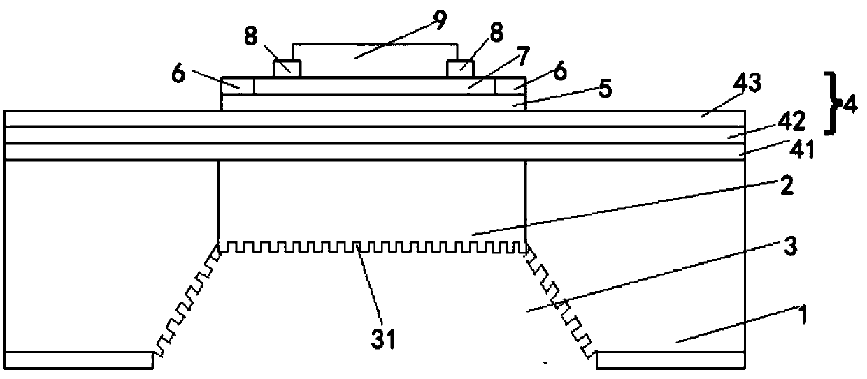
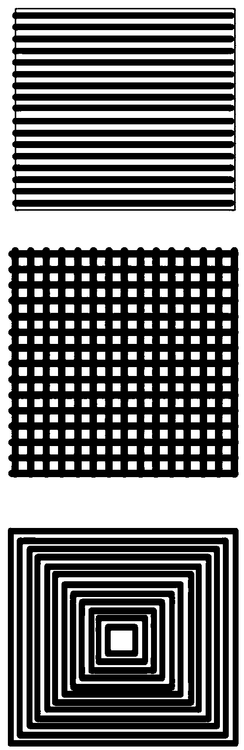
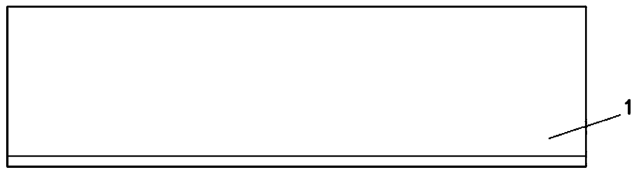
[0031] Example 1: figure 1 It is a structural schematic diagram of the MEMS gas sensor of the present invention, and it can be clearly seen from the figure that the MEMS gas sensor of the present invention includes: a single crystal silicon substrate 1; a porous silicon layer 2, which is formed on the surface of the single crystal silicon substrate 1 The upper surface has a thickness downward, and a silicon dioxide film is formed on the upper surface and the surface of the hole wall of the porous silicon layer 2; the heat insulating groove 3 is formed on the lower surface of the single crystal silicon substrate 1, and the heat insulating The groove 3 is an undercut groove, the bottom surface of the heat insulating groove 3 is located directly below the porous silicon layer 2, and the wall and bottom surface of the heat insulating groove 3 are provided with one or more groove groups, wherein each groove group includes A plurality of trenches 31 arranged in parallel; the lower i...

Embodiment 2

[0050] Example 2: figure 1 It is a structural schematic diagram of the MEMS gas sensor of the present invention, and it can be clearly seen from the figure that the MEMS gas sensor of the present invention includes: a single crystal silicon substrate 1; a porous silicon layer 2, which is formed on the surface of the single crystal silicon substrate 1 The upper surface has a thickness downward, and a silicon dioxide film is formed on the upper surface and the surface of the hole wall of the porous silicon layer 2; the heat insulating groove 3 is formed on the lower surface of the single crystal silicon substrate 1, and the heat insulating The groove 3 is an undercut groove, the bottom surface of the heat insulating groove 3 is located directly below the porous silicon layer 2, and the wall and bottom surface of the heat insulating groove 3 are provided with one or more groove groups, wherein each groove group includes A plurality of trenches 31 arranged in parallel; the lower i...

Embodiment 3

[0069] Example 3: figure 1 It is a structural schematic diagram of the MEMS gas sensor of the present invention, and it can be clearly seen from the figure that the MEMS gas sensor of the present invention includes: a single crystal silicon substrate 1; a porous silicon layer 2, which is formed on the surface of the single crystal silicon substrate 1 The upper surface has a thickness downward, and a silicon dioxide film is formed on the upper surface and the surface of the hole wall of the porous silicon layer 2; the heat insulating groove 3 is formed on the lower surface of the single crystal silicon substrate 1, and the heat insulating The groove 3 is an undercut groove, the bottom surface of the heat insulating groove 3 is located directly below the porous silicon layer 2, and the wall and bottom surface of the heat insulating groove 3 are provided with one or more groove groups, wherein each groove group includes A plurality of trenches 31 arranged in parallel; the lower i...


PUM

PropertyMeasurementUnit
thicknessaaaaaaaaaa
thicknessaaaaaaaaaa
thicknessaaaaaaaaaa

Abstract

The invention relates to the technical field of gas detection, and in particular relates to an MEMS gas sensor. The MEMS gas sensor comprises a monocrystalline silicon substrate, a porous silicon layer which is formed on the upper surface of the monocrystalline silicon substrate and has thickness downwards, a heat insulation trough formed on the lower surface of the monocrystalline silicon substrate in an inverse manner, a lower insulation layer, a heating layer, an upper insulation layer and a gas sensitive layer, wherein the bottom surface of the heat insulation trough is positioned just under the porous silicon layer; the heat insulation trough comprises one or multiple trench groups; the lower insulation layer covers the porous silicon layer and the upper surface of the monocrystalline silicon substrate and comprises a first silicon dioxide layer, a second silicon dioxide layer and a silicon nitride layer from bottom to top in sequence; the heating layer, the upper insulation layer and the gas sensitive layer are arranged above the lower insulation layer. The invention also correspondingly discloses a manufacturing method of the MEMS gas sensor. By virtue of the structures of porous silicon and the heat insulation trough, the heat insulation effect is enhanced; the lower insulation layer effectively prevents the heat insulation layer warping to break away from the heating layer at high temperature; meanwhile, under the supporting of the porous silicon layer, deformation and cracks, which are caused by non-uniform stress, of the lower insulation layer are prevented, and thus the service life of the gas sensor is prolonged.

Description

technical field [0001] The invention relates to the technical field of gas detection, in particular to a MEMS gas sensor and a manufacturing method thereof. Background technique [0002] The various environments of human production, living and living are filled with various gases. The detection of gases, especially the detection of toxic, harmful, flammable and explosive gases, is an important means to ensure people's safe production, healthy living and comfortable life. At present, there are traditional large-scale detection equipment for gas detection, such as gas detection instruments based on mass spectrometry, energy spectroscopy and chromatography, but these instruments are bulky and expensive, which limits their popularization and development. Therefore, some small gas sensors have been developed in recent years. Gas sensors are widely used in petroleum, petrochemical, gas, metallurgy, electric power, automobile industry, environmental sanitation, meteorological detec...

Claims


Application Information

Patent Timeline
Patent Type & Authority Applications(China)
IPC IPC(8): G01N27/00B81B7/00B81C1/00
Inventor 祁明锋张珽沈方平刘瑞丁海燕谷文
Owner SUZHOU LEANSTAR ELECTRONICS TECH
Why Eureka
Try Eureka