

Simulation technique based semiconductor device TDDB (time dependent dielectric breakdown) failure testing method
A semiconductor and device technology, applied in the field of TDDB failure testing of semiconductor devices based on simulation technology, can solve the problems of impurity diffusion, pre-test preparation time of expensive test equipment, diffusion into silicon substrate or fixed in silicon dioxide, etc. Time and cost saving effect
- Summary
- Abstract
- Description
- Claims
- Application Information
AI Technical Summary
Problems solved by technology
Method used
Image

Examples
Embodiment Construction
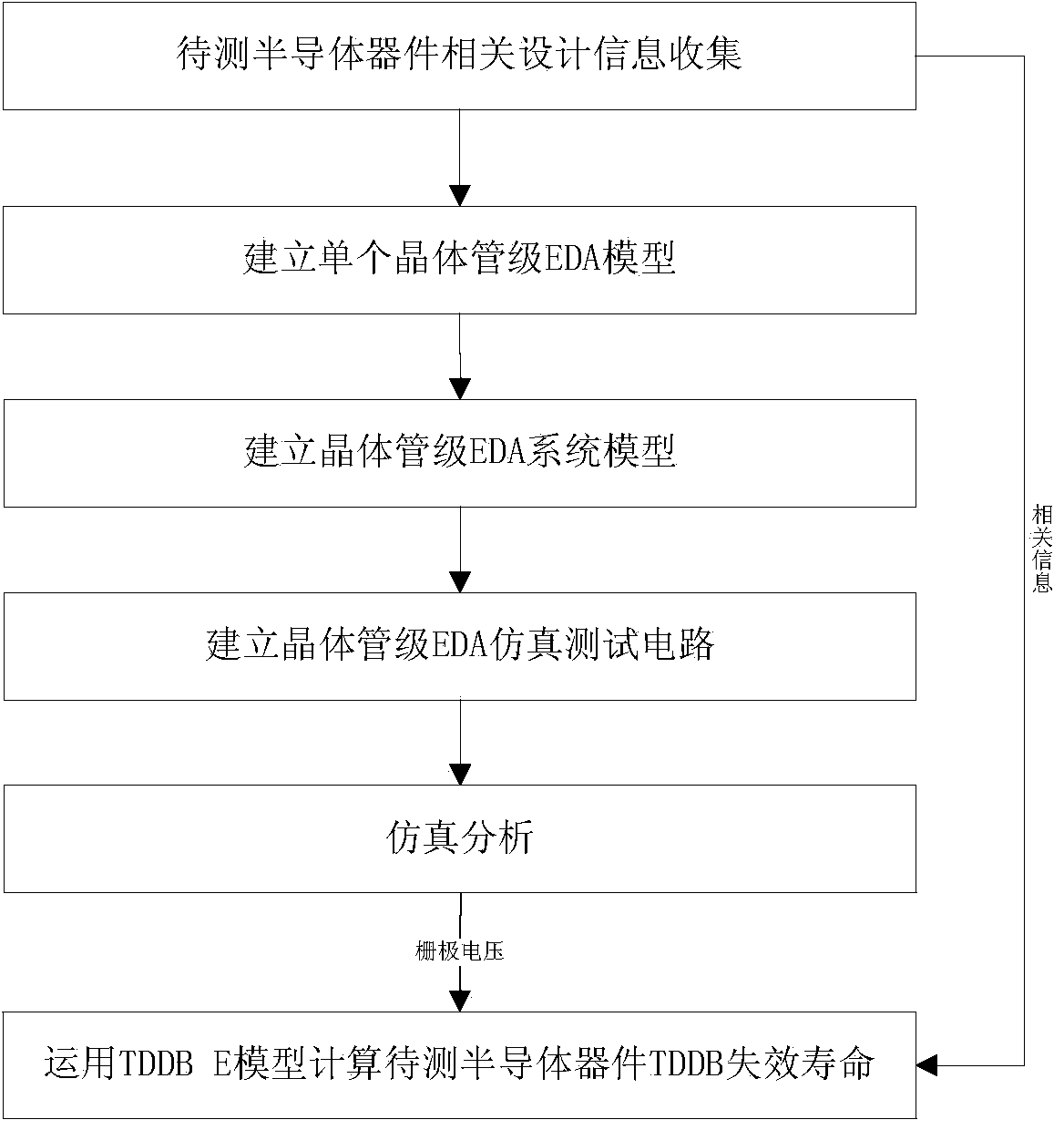
[0022] The technical solution of the present invention will be described in further detail below in conjunction with the accompanying drawings:
[0023] Taking "CD4011B" as an example below, the TDDB failure test method for semiconductor devices based on simulation technology described in the present invention is introduced. figure 1 As shown, the steps of this method are:
[0024] Step 1: Collect the known information of "CD4011B", including:
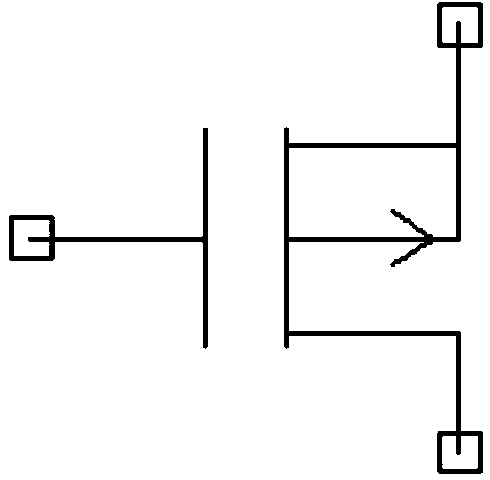
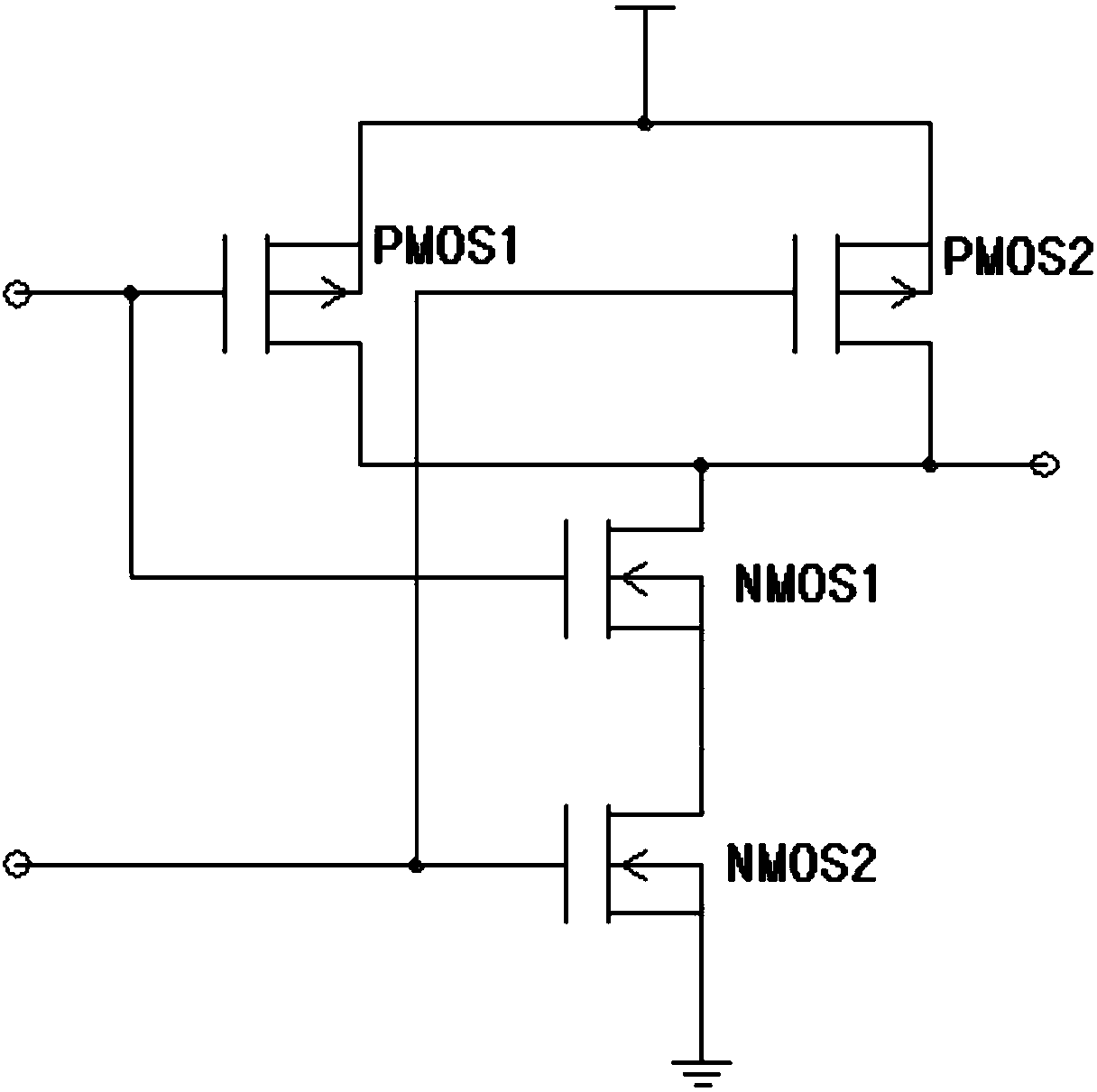
[0025] a) "CD4011B" internal transistor level circuit diagram;
[0026] b) "CD4011B" internal transistor gate oxide breakdown activation energy, electric field breakdown coefficient and electric field acceleration factor;
[0027] c) "CD4011B" internal transistor gate oxide layer thickness;
[0028] d) "CD4011B" internal transistor channel design length, effective width, source area, drain area and other information;
[0029] e) The typical application circuit of the device provided by the "CD4011B" manufacturer, which includes the...
PUM
 Abstract
Description
Claims
Application Information