Electric-fuse structures and formation methods thereof, and semiconductor devices and formation methods thereof

A technology of electric fuses and semiconductors, applied in semiconductor devices, semiconductor/solid-state device manufacturing, semiconductor/solid-state device components, etc., can solve the problem of single forming method, and achieve the effect of simple forming method and novel structure

Active Publication Date: 2014-12-03
SEMICON MFG INT (SHANGHAI) CORP
View PDF7 Cites 25 Cited by
  • Summary
  • Abstract
  • Description
  • Claims
  • Application Information

AI Technical Summary

Problems solved by technology

[0009] However, the electric fuse structure and its forming method formed in the prior art are single, and the electric fuse is usually formed when forming a planar transistor. How to realize the diversification of the electric fuse structur

Method used


Image

  • Electric-fuse structures and formation methods thereof, and semiconductor devices and formation methods thereof
  • Electric-fuse structures and formation methods thereof, and semiconductor devices and formation methods thereof
  • Electric-fuse structures and formation methods thereof, and semiconductor devices and formation methods thereof

Examples


no. 1 example

[0077] In the first embodiment of the present invention, the inventor provides a method and structure for forming an electric fuse when forming a gate-all-around transistor.

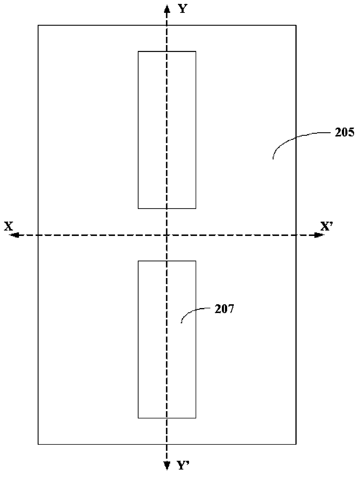
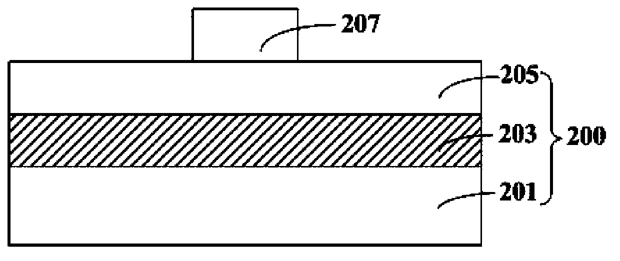
[0078] Please refer to Figure 2A , 2B , 2C, where, Figure 2A It is a schematic top view structure diagram of the formation process of the semiconductor device according to the first embodiment of the present invention, Figure 2B for Figure 2A Schematic diagram of the cross-sectional structure along the X-X' direction; Figure 2C for Figure 2A Schematic diagram of the cross-sectional structure along the Y-Y' direction.

[0079] It should be noted that, in order to facilitate the understanding of the present invention, in the embodiments of the present invention, the schematic cross-sectional structure along the X-X' direction only shows the structure on the cross-section.

[0080] Provide a semiconductor-on-insulator substrate (SOI) 200 including a first region I and a second region II, wherein...

no. 2 example

[0149] Different from the first embodiment, in the second embodiment of the present invention, a method for forming an electric fuse structure is provided. The electric fuse structure does not necessarily have to be parasitic in the formation step of the gate-enclosed transistor, and can be independently Formation of electrical fuse structures on nanowires on semiconductor substrates.

[0150] Please refer to Figure 16 , provide a semiconductor-on-insulator substrate, the semiconductor-on-insulator substrate includes a back substrate 301, a buried oxide layer 303 covering the surface of the back substrate 301, and a top semiconductor layer (not shown) covering the surface of the buried oxide layer 303 mark); etch the top semiconductor layer to form a suspended nanowire 305f, which is used to form an electric fuse structure including a cathode 323, an anode 325 and a fusing region; doping at both ends of the nanowire 305 The cathode 323 and the anode 325 forming the electric ...

no. 3 example

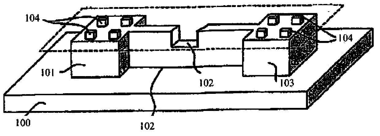
[0164] Different from the first and second embodiments of the present invention, in the third embodiment of the present invention, the electric fuse structure is formed at the same time as the FinFET. Moreover, the process of the fin field effect transistor in the first region is divided into a process of forming the high-k gate dielectric layer before (HK First) and a process of forming the high-k gate dielectric layer after (HK Last). In the third embodiment of the present invention, the electric fuse structure is formed during the process of forming the high-k gate dielectric layer first.

[0165] Please refer to Figure 17 and Figure 18 , wherein, FIG. 17 is a schematic diagram of a three-dimensional structure of a semiconductor device formation process, Figure 18 It is a schematic cross-sectional structure diagram along the direction A-A1 in FIG. 17 .

[0166] Firstly, a semiconductor substrate 400 is provided, the semiconductor substrate 400 includes a first region I'...


PUM


Abstract

The embodiment of the invention provides a plurality of kinds of electric-fuse structures and formation methods thereof, and semiconductor devices and formation methods thereof, e.g., doping is carried out in a nanowire or a fin part so that an electric-fuse structure is formed and while a full-surrounding gate transistor or a fin-type field effect transistor is formed, a corresponding electric-fuse structure is formed at the same time and thus diversity of the electric-fuse structures and the semiconductor devices is realized. And when a step of forming the electric-fuse structure parasitizes in a step of forming the full-surrounding gate transistor or the fin-type field effect transistor, no extra process step is added so that production cost is low.

Description

technical field [0001] The invention relates to the technical field of semiconductor manufacturing, in particular to an electric fuse structure and its forming method, a semiconductor device and its forming method. Background technique [0002] In the field of integrated circuits, fuses (Fuse) refer to some fuseable connection lines formed in integrated circuits. Initially, fuses are used to connect redundant circuits in integrated circuits. Once the integrated circuits are found to be defective, the fuses are used to repair or replace the defective circuits. There are generally two types of fuses: laser fuse (Laser Fuse) and electrical fuse (Electrical Fuse, hereinafter referred to as E-fuse). With the development of semiconductor technology, E-fuse has gradually replaced laser fuse. [0003] Generally, the electric fuse structure can be made of metal (aluminum, copper, etc.) or silicon. A typical electric fuse structure in the prior art is as figure 1 As shown, the elec...

Claims


Application Information

Patent Timeline
IPC IPC(8): H01L21/768H01L23/525
CPCB82Y40/00H01L21/768H01L21/76886H01L21/76888H01L23/5256H01L23/528H01L29/66484H01L29/66795H01L29/7831H01L29/785
Inventor 李勇
Owner SEMICON MFG INT (SHANGHAI) CORP
Why Eureka
Try Eureka