Production process of super-junction device

A preparation process and technology for superjunction devices, applied in the field of superjunction device preparation technology, can solve the problems of N/P charge unbalanced breakdown voltage, difficult to achieve, and voids at the bottom of trenches, so as to reduce filling difficulty and defects The effect of forming, increasing the breakdown voltage, and reducing the difficulty of etching

Active Publication Date: 2014-12-10
CHINA RESOURCES MICROELECTRONICS (CHONGQING) CO LTD
View PDF3 Cites 3 Cited by
  • Summary
  • Abstract
  • Description
  • Claims
  • Application Information

AI Technical Summary

Problems solved by technology

[0005] And these put forward very high requirements on the manufacturing process, which is generally difficult to achieve
In particular, it is necessary to further reduce the cell size to achieve a smaller Rsp, and the general manufacturing process can only be prohibitive
[0006] Due to the deep depth of the groove prepared, it is necessary to use DRIE (Deep Reactive Ion Etching, deep reactive ion etching) equipment for etching. At present, the cost of DRIE equipment is very expensive, which undoubtedly increases the production cost and preparation difficulty; at the same time Due to the relatively large depth-width ratio of the prepared trench, during the process of filling the trench with the P-type epitaxial layer 3, the P-type epitaxial layer 3 may form a blockage at the opening, causing a cavity 4 to be formed at the bottom of the trench, such as Figure 2f As shown, this will have an adverse effect on device performance; furthermore, because it is difficult to make the trench side wall absolutely straight, the traditional trench-SJ often has a very narrow bottom, which causes the N / P charge imbalance to cause breakdown voltage drop

Method used


Image

  • Production process of super-junction device
  • Production process of super-junction device
  • Production process of super-junction device

Examples


Embodiment 1

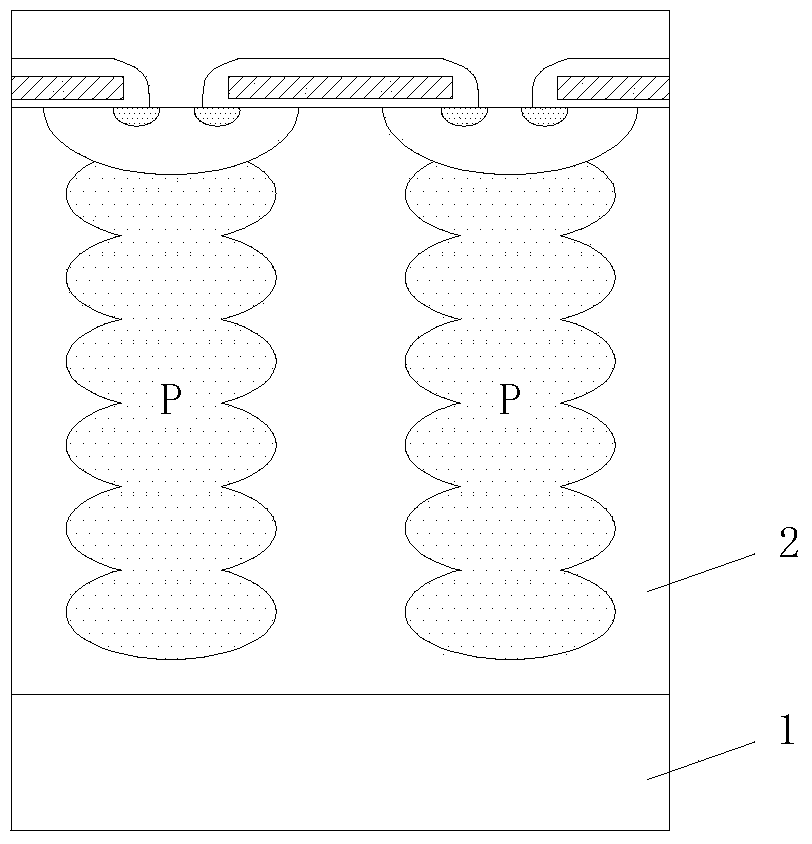
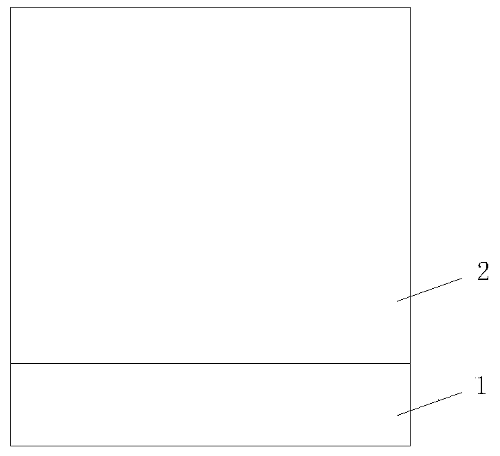
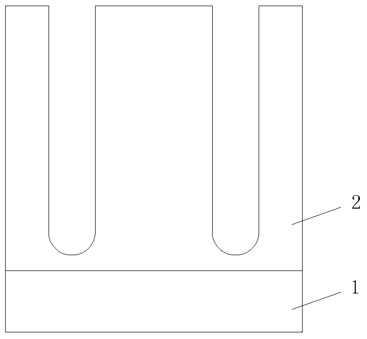
[0038] Step S1: Provide a substrate 10, grow multiple epitaxial layers with the first conductivity type sequentially from bottom to top on the top of the substrate 10, and after forming each epitaxial layer, etch the epitaxial layer to form several spaced apart trenches, and then filling the trenches with a semiconductor layer of the second conductivity type, wherein the trenches formed in any two upper and lower adjacent epitaxial layers correspond to each other and overlap up and down.

[0039] In this embodiment, the above-mentioned first conductivity type is an N-type conductivity type, and the second conductivity type is a P-type conductivity type.

[0040] In the present invention, firstly, a first layer of epitaxial layer (N-type conductivity type) 11 with a thicker thickness and lower doping is formed on a substrate 10 provided by an epitaxial growth process, and then through a substrate with an opening The patterned mask layer etches the first epitaxial layer 11 to fo...

Embodiment 2

[0051] Step S1: Provide a substrate 50, first deposit a buffer layer 51 with the second conductivity type on the upper surface of the substrate 50, and then grow multiple layers of the first conductivity type sequentially on the buffer layer 51 from bottom to top. epitaxial layer, and after each epitaxial layer is formed, the epitaxial layer is etched to form a plurality of spaced apart trenches 60, and then the trenches 60 are filled with a semiconductor layer of the second conductivity type, wherein any The trenches formed in the epitaxial layers adjacent to each other up and down correspond to each other and overlap up and down.

[0052] In this embodiment, the above-mentioned first conductivity type is a P-type conductivity type, and the second conductivity type is an N-type conductivity type.

[0053] Specifically, an N-type buffer layer 51 is first formed on the substrate 50, and then a first layer of epitaxial layer 52 with P-type heavy doping is sequentially deposited ...


PUM


Abstract

The invention discloses a production process of a super-junction device. Trenches are etched and filled to form a super-junction. Each trench is etched section by section, so that etching difficulty is greatly reduced, and the sidewall of the trench is more vertical. During a filling process, a depth-to-width ratio of each trench is small, so that filling difficulty is greatly reduced and defects are greatly lessened; meanwhile, by the use of the sectional process, charge balance can be easily maintained for all positions, and breakdown voltage is increased. In addition, by the use of sectional process, the quantity of electric charge can be locally changed, and more device feature optimization methods are provided for designers.

Description

technical field [0001] The invention relates to the field of semiconductors, in particular to a preparation process of a super junction device. Background technique [0002] Super-Junction (SJ, super junction) transistor is a unique N / P interactive structure, so that only thinner EPI (epitaxial layer) and higher EPI doping are required under the same breakdown voltage, thus greatly reducing the The specific on-resistance of the device-Rsp, and the figure of merit (FOM, quality factor) value. [0003] At present, the Super-Junction is usually formed by multiple epitaxy + implantation + annealing. However, this method causes the concentration of local P-pillars to be too high, which easily leads to premature breakdown, such as figure 1 As shown, P columns are formed in the composite epitaxial layer 2 formed by multi-layer epitaxial layers prepared on the substrate 1. At the same time, because the concentration and area of ​​the effective N columns are reduced due to the need...

Claims


Application Information

Patent Timeline
Patent Type & Authority Applications(China)
IPC IPC(8): H01L21/3065H01L21/20H01L29/06
CPCH01L29/0634
Inventor 马荣耀可瑞思
Owner CHINA RESOURCES MICROELECTRONICS (CHONGQING) CO LTD
Why Eureka
Try Eureka