Efficient GaN-based LED coupled to plasmon and manufacturing method thereof

A plasma and exciton technology, applied in electrical components, semiconductor devices, circuits, etc., can solve problems such as influence, improve near-field coupling efficiency, improve SPP wavelength excitation consistency and controllability, and improve device internal quantum The effect of efficiency

Inactive Publication Date: 2014-12-17
TIANJIN POLYTECHNIC UNIV
View PDF5 Cites 9 Cited by
  • Summary
  • Abstract
  • Description
  • Claims
  • Application Information

AI Technical Summary

Problems solved by technology

However, the disadvantage of using metal nanoparticles to enhance the luminous efficiency of GaN-LEDs is that this metho...

Method used


Image

  • Efficient GaN-based LED coupled to plasmon and manufacturing method thereof
  • Efficient GaN-based LED coupled to plasmon and manufacturing method thereof

Examples


Embodiment Construction

[0029] In order to achieve the above object, the technical scheme adopted in the present invention is:

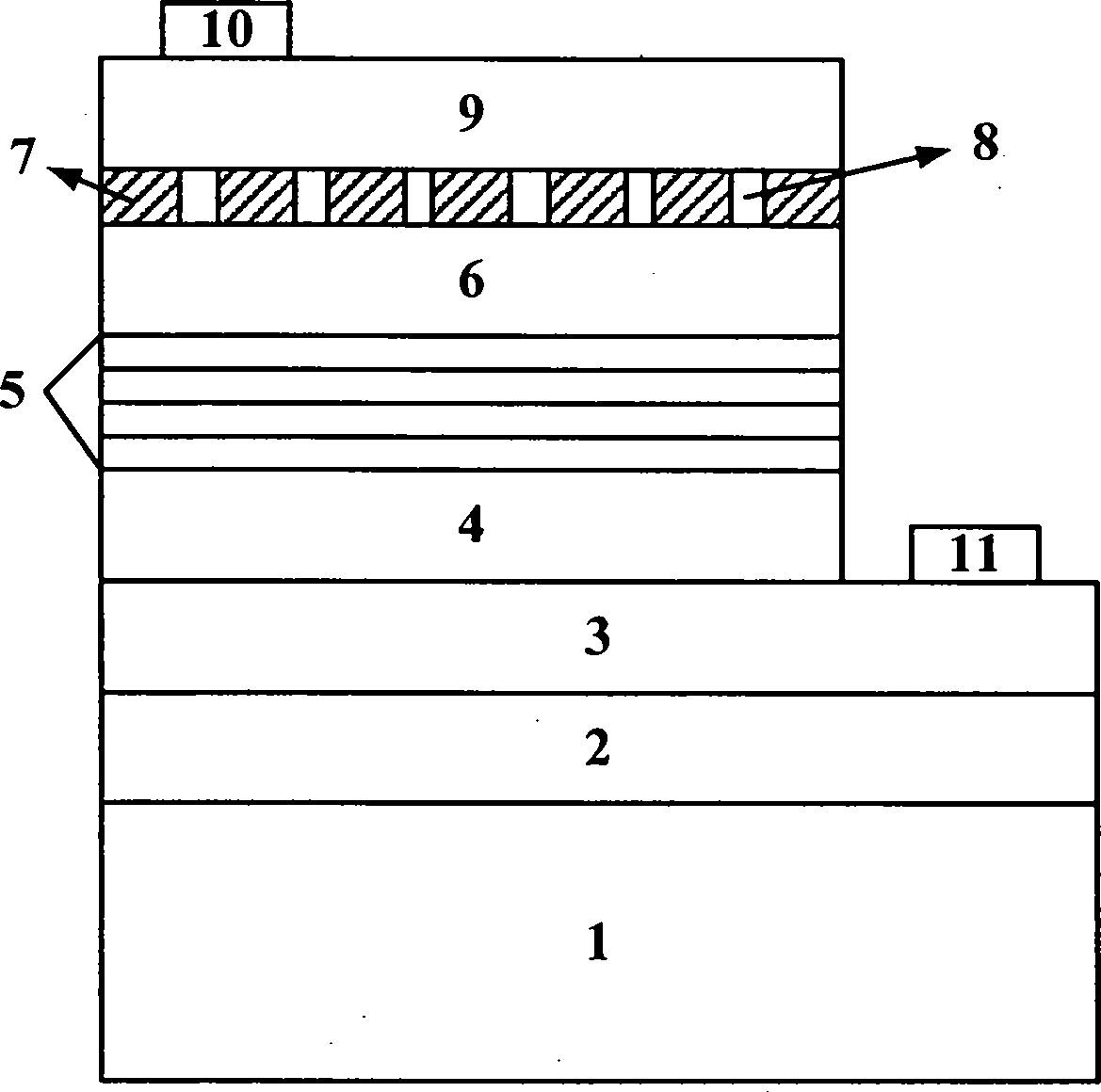
[0030] A high-efficiency GaN-based LED coupled with plasmons (as attached figure 1 Shown), its preparation method specifically comprises the following steps:

[0031] (1) The GaN-based LED is grown on a sapphire substrate by metal-organic chemical vapor deposition;

[0032] (2) In an environment of 550°C, grow a GaN nucleation layer with a thickness between 23nm and 27nm on a sapphire substrate;

[0033] (3) Raise the temperature to 1020°C, and grow a GaN undoped layer and an n-type GaN layer with a thickness between 1900nm and 2100nm, respectively;

[0034] (4) Lower the temperature to 770°C and re-grow InGaN / GaN multiple quantum wells with a cycle number of 4-6;

[0035] (5) Raise the temperature to 970°C, and re-grow a p-type GaN ohmic contact layer with a thickness between 27nm and 33nm;

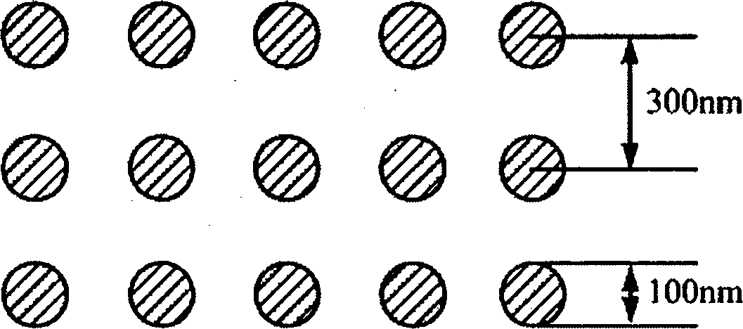
[0036] (6) On the p-type GaN, an Ag layer is prepared by using an electron be...


PUM

PropertyMeasurementUnit
Thicknessaaaaaaaaaa
Thicknessaaaaaaaaaa
Thicknessaaaaaaaaaa

Abstract

The invention belongs to the technical field of microelectronics and optoelectronics and relates to an efficient GaN-based LED coupled to a plasmon and a manufacturing method thereof. The efficient GaN-based LED comprises a sapphire substrate, a GaN nucleating layer, a GaN undoped layer, an n-type GaN layer, InGaN/GaN multiple quantum wells, a p-type GaN ohmic contact layer, an Ag photonic crystal layer and a p-type GaN doped layer. Gaps of Ag photonic crystal are filled with p-type GaN. One electrode P and one electrode N are provided. The efficient GaN-based LED is manufactured by a MOCVD (metal organic chemical vapor deposition) technology and a micro-nano machining technology, and luminous efficiency of a device is enhanced by local coupling of SPP (surface plasmon polartions) leak mode and near field of the metal photonic crystal.

Description

technical field [0001] The invention relates to the technical fields of microelectronics and optoelectronics, in particular to a GaN-based LED with high photoelectric conversion efficiency and a manufacturing method thereof. The invention utilizes the plasmon polariton (Surface Plasmon Polaritcn, SPP) mode coupling of the two-dimensional metallic Ag photonic crystal to enhance the luminous efficiency of the GaN-based light-emitting diode. Background technique [0002] III-V compound semiconductor materials are widely used in the field of light emission, and GaN has been identified as one of the best materials for making high-efficiency light-emitting diodes. With the rapid development of the semiconductor lighting industry, the demand for high-efficiency LED chips continues to grow, and further improving the luminous efficiency of GaN-LEDs is still a hot issue in the scientific community. Among the many ways to enhance the luminous efficiency of LEDs, the use of surface pla...

Claims


Application Information

Patent Timeline
IPC IPC(8): H01L33/06H01L33/02H01L33/32H01L33/00
CPCH01L33/06H01L33/0075H01L33/02H01L33/32H01L2933/0008H01L2933/0066
Inventor 刘宏伟刘春影杨华杨广华阚强陈弘达
Owner TIANJIN POLYTECHNIC UNIV
Why Eureka
Try Eureka