Metal plasmon coupling luminescence enhancement silicon substrate LED and manufacturing method thereof

A metal plasma and luminescence enhancement technology, applied in electrical components, semiconductor devices, circuits, etc., can solve the problems of large differences in properties such as plasmon resonance frequency SPP absorption and scattering, etc., and achieve good SPP wavelength excitation consistency and controllability performance, improve the quantum efficiency of the device, and improve the effect of near-field coupling efficiency

Inactive Publication Date: 2014-02-05
TIANJIN POLYTECHNIC UNIV
View PDF4 Cites 8 Cited by
  • Summary
  • Abstract
  • Description
  • Claims
  • Application Information

AI Technical Summary

Problems solved by technology

The common structure in SPP is metal thin film or metal island film with nanostructure, but due to the fine structure of the metal film (such as metal particle size, particle distribution, particle shape, particle volume fraction, particle composition and particle structure, etc.) Different, the plasmon resonance frequency, SPP absorption and scattering properties are quite different, and the results after interacting with the luminescent center are also different.

Method used


Image

  • Metal plasmon coupling luminescence enhancement silicon substrate LED and manufacturing method thereof
  • Metal plasmon coupling luminescence enhancement silicon substrate LED and manufacturing method thereof
  • Metal plasmon coupling luminescence enhancement silicon substrate LED and manufacturing method thereof

Examples


Embodiment Construction

[0038] The present invention will be further described below with reference to the drawings and embodiments.

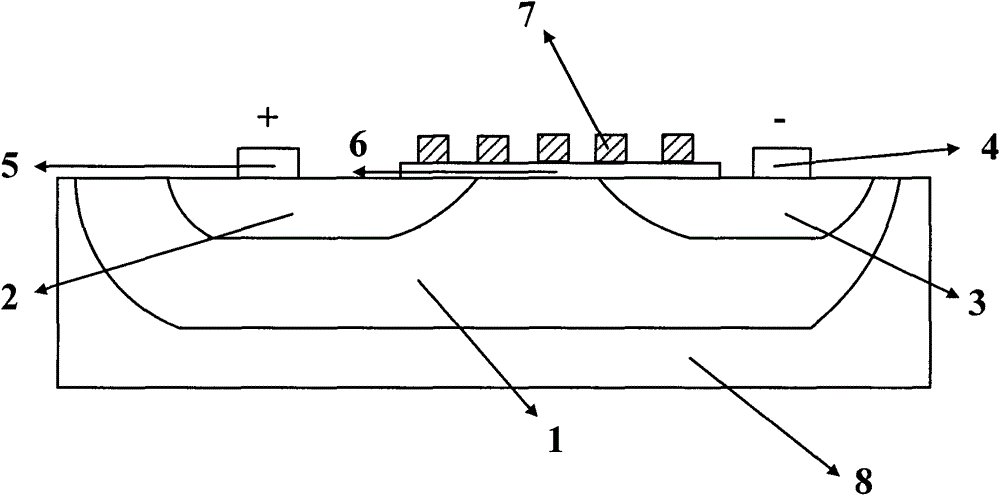
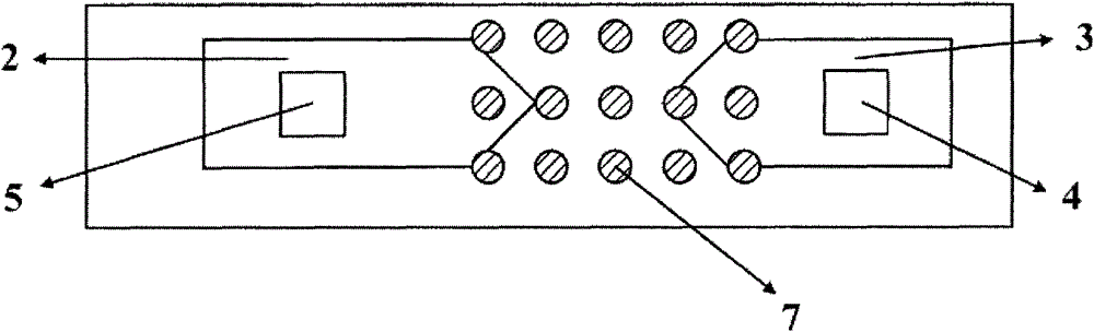
[0039] The LED produced by the present invention is prepared by referring to the CMOS process to prepare a wedge-shaped electrode shallow well electroluminescent PN junction. + A layer of SiO is prepared on the N-well light-emitting junction 2 . In SiO 2 On top, a layer of metal photonic crystal is prepared. As attached figure 1 And figure 2 Shown.

[0040] The invention refers to the standard integrated circuit process, and designs the plasmon coupling to enhance the light emission of the device. The PN junction of the device is designed in a shallow well, and the carriers are located on the surface of the device to recombine, reducing the absorption of light radiation by silicon-based materials. PMOS and NMOS source and drain region ion implantation processes are used to inject P+ and N+ wedge-shaped electrodes to generate a PN junction to inject a strong electric fie...


PUM

PropertyMeasurementUnit
thicknessaaaaaaaaaa

Abstract

The invention belongs to the technical field of micro-electronics and photoelectronics, and relates to a metal plasmon coupling luminescence enhancement silicon substrate LED which is manufactured based on the standard CMOS technique. The metal plasmon coupling luminescence enhancement silicon substrate LED comprises a P electrode, an N electrode and a P+N trap light-emitting junction which is integrated on a P type silicon substrate. The P+ and N+ are of a wedge structure with the tip angle ranging from 75 degrees to 90 degrees, a layer of SiO2 covers the P+N trap light-emitting junction at first, and then a metal Ag photonic crystal structure is manufactured on the surface of the SiO2. The light-emitting efficiency of a device is enhanced through the SPP leakage mode near field local coupling of a metal photonic crystal, the light-emitting strength of the silicon substrate CMOS device is improved, the light-emitting area of the device is centralized, the device has high light power density, and the photoelectricity integration of the device is facilitated.

Description

Technical field [0001] The invention relates to the technical field of microelectronics and optoelectronics, in particular to a silicon-based LED with high photoelectric conversion efficiency. The invention utilizes the optimized device structure and the plasmon (Surface Plasmon Polariton, SPP) mode coupling of the two-dimensional metal photonic crystal to enhance the luminous efficiency of the silicon-based light-emitting diode. Background technique [0002] In recent years, the use of the plasmonic coupling of the metal dielectric nanoparticle structure in the device to achieve luminescence enhancement is an effective method to enhance the performance of light-emitting devices that is currently paid much attention at home and abroad. [0003] In 2006, the Pillai research team in Australia used a Silicon-on-insulator (SOI) LED with a silver nanoparticle layer to excite the SPP of silver nanoparticles to increase the electroluminescence efficiency of 900nm by 8 times. [0004] In 20...

Claims


Application Information

Patent Timeline
Patent Type & Authority Applications(China)
IPC IPC(8): H01L33/38H01L33/44H01L33/00
CPCH01L33/24H01L33/0054H01L33/44
Inventor 刘宏伟刘春影杨广华王真真阚强陈弘达
Owner TIANJIN POLYTECHNIC UNIV
Why Eureka
Try Eureka