Organic light emission diode device and fabrication method thereof

An electroluminescence device and electroluminescence technology, which are applied in the directions of organic semiconductor devices, materials of organic semiconductor devices, and electric solid devices, etc., can solve the problem of high manufacturing cost, the polarizing film is easily affected by humidity and ambient temperature, and the brightness of light output is low. And other issues

Inactive Publication Date: 2014-12-17
OCEANS KING LIGHTING SCI&TECH CO LTD +2
View PDF5 Cites 6 Cited by
  • Summary
  • Abstract
  • Description
  • Claims
  • Application Information

AI Technical Summary

Problems solved by technology

Since the reflective electrode at the bottom is generally made of a metal electrode, which has a high reflectivity, the external ambient light will also be strongly reflected on the bottom electrode, which makes the OLED device have low contrast and display clarity, and the top-emitting

Method used


Image

  • Organic light emission diode device and fabrication method thereof
  • Organic light emission diode device and fabrication method thereof
  • Organic light emission diode device and fabrication method thereof

Examples


Embodiment 1

[0060] A method for preparing an organic electroluminescent device, comprising the following steps:

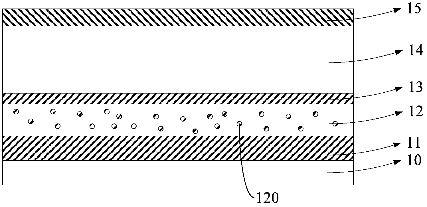
[0061] (1) Place the glass substrate on a 1×10 -4 In the vacuum coating chamber of Pa, a metal Ag film with a thickness of 500nm was prepared on the surface of the substrate by vacuum evaporation as a reflective electrode;

[0062] (2) A light-scattering layer with a thickness of 100 μm is formed on the surface of the reflective electrode by a screen printing process. The material of the light-scattering layer includes titanium dioxide nanospheres and photocurable acrylic resin with a mass ratio of 50:100. The particle size is 50nm, and the screen printing process uses screen printing with a mesh number of 200 to form a film;

[0063] (3) A layer of ITO film with a thickness of 200nm was sputtered on the surface of the light scattering layer by magnetron sputtering as the first transmission electrode, and the sputtering speed was 0.2nm / s; Prepare a light-emitting functional ...

Embodiment 2

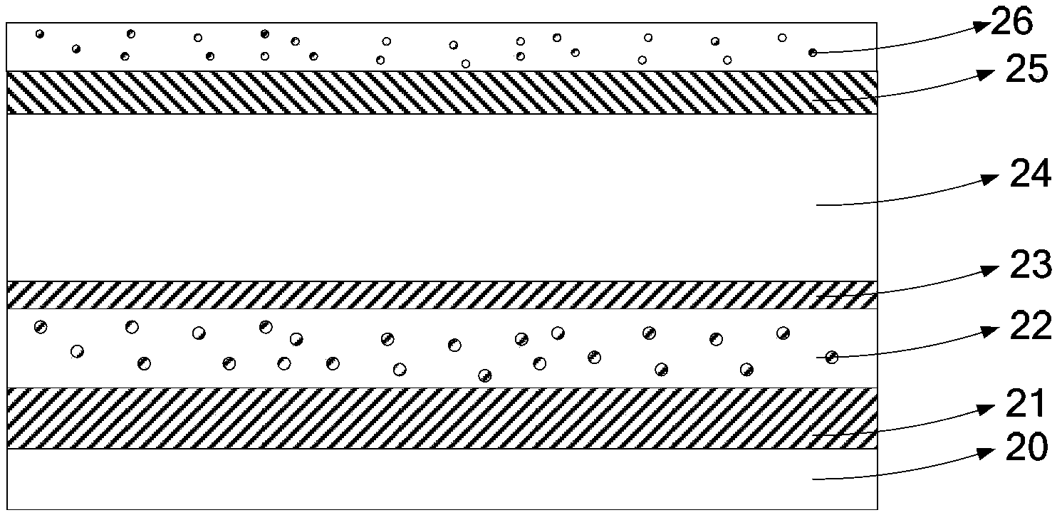
[0068] The difference between this embodiment and Embodiment 1 is that the material of the light scattering layer includes titanium dioxide nano-microspheres and photocurable acrylic resin with a mass ratio of 20:100, the particle size of the titanium dioxide nano-microspheres is 100nm, and the screen printing process adopts mesh A film was formed by screen printing with a mesh of 1000, and the thickness of the light scattering layer was 80 μm.

Embodiment 3

[0070] The difference between this embodiment and Embodiment 1 is that the material of the light scattering layer includes titanium dioxide nano-microspheres and photocurable acrylic resin with a mass ratio of 20:100, the particle size of the titanium dioxide nano-microspheres is 250nm, and the screen printing process adopts a mesh A film was formed by screen printing with a mesh of 400, and the thickness of the light scattering layer was 20 μm.


PUM

PropertyMeasurementUnit
Particle sizeaaaaaaaaaa
Thicknessaaaaaaaaaa
Meshaaaaaaaaaa

Abstract

The invention provides an organic light emission diode device. The organic light emission diode device comprises a substrate and a reflection layer, a light scattering layer, a first transmitting electrode, a light emission functional layer and a second transmitting electrode which are sequentially laminated on the substrate, the material of the light scattering layer comprises nanoparticles and a polymer material, the nanoparticles are ceramic or high-polymer material particles with grain size of 50 to 1,500 nanometers, the polymer material is a heat cured polymer or photo cured polymer material, the thickness of the light scattering layer is 10 to 100 micrometers, the material of the reflection electrode is a metal membrane, and the metal membrane comprises metal elemental gold, silver, aluminum, copper, nickel, platinum and magnesium or an alloy formed by any combination thereof. In the organic light emission diode device, through the arrangement of the light scattering layer on the surface of the reflection electrode, the reflectivity of the device is greatly reduced, so that the contrast of the device is improved. The invention also provides a fabrication method of the organic light emission diode device.

Description

technical field [0001] The invention relates to an organic electroluminescent device, in particular to an organic electroluminescent device and a preparation method thereof. Background technique [0002] Organic Light Emission Diode, hereinafter referred to as OLED, has the characteristics of high brightness, wide range of material selection, low driving voltage, fully cured active light emission, etc., and has the advantages of high definition, wide viewing angle, and fast response speed. It is a display technology and light source with great potential, which conforms to the development trend of mobile communication and information display in the information age, as well as the requirements of green lighting technology, and is the focus of many researchers at home and abroad. [0003] In the existing top-emitting OLED light-emitting device, light is generally reflected by the reflective electrode at the bottom, and then emitted from the transmissive electrode at the top. S...

Claims


Application Information

Patent Timeline
IPC IPC(8): H01L51/52H01L51/54H01L51/56H01L51/50
CPCH10K50/854H10K50/856H10K2102/00H10K71/00
Inventor 周明杰冯小明黄辉王平
Owner OCEANS KING LIGHTING SCI&TECH CO LTD
Why Eureka
Try Eureka