Wave aberration detection device of objective lens imaging system and system error correction method of wave aberration detection device

The technology of an imaging system and a detection device, which is applied in the field of optical measurement, can solve the problems such as the reduction of the accuracy of the wavefront sensor in detecting the wave aberration of the objective lens, and achieve the effects of simple structure, convenient installation and adjustment, and simple calibration scheme

Active Publication Date: 2014-12-24
SHANGHAI INST OF OPTICS & FINE MECHANICS CHINESE ACAD OF SCI
View PDF10 Cites 37 Cited by
  • Summary
  • Abstract
  • Description
  • Claims
  • Application Information

AI Technical Summary

Problems solved by technology

Due to the existence of these system errors, the accuracy of the wavefront sensor to detect the wave aberration of the objective lens is greatly reduced

Method used


Image

  • Wave aberration detection device of objective lens imaging system and system error correction method of wave aberration detection device
  • Wave aberration detection device of objective lens imaging system and system error correction method of wave aberration detection device
  • Wave aberration detection device of objective lens imaging system and system error correction method of wave aberration detection device

Examples


Embodiment Construction

[0025] In order to better understand the purpose, technical solutions and advantages of the embodiments of the present invention, the present invention will be further described below in conjunction with the accompanying drawings and embodiments, but the protection scope of the present invention should not be limited thereby.

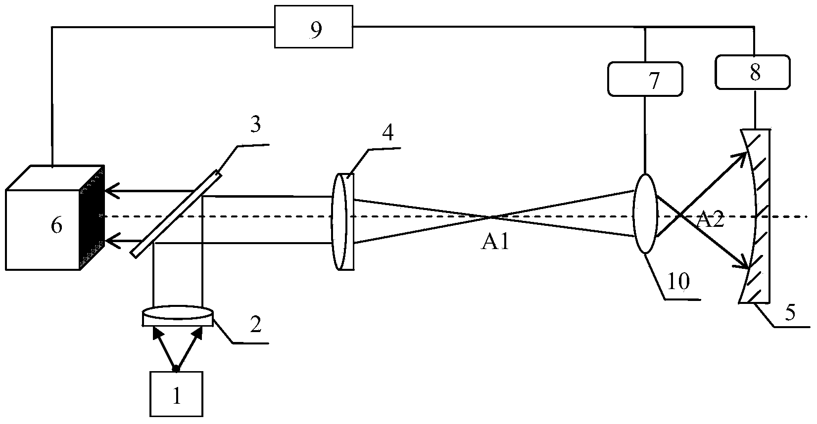
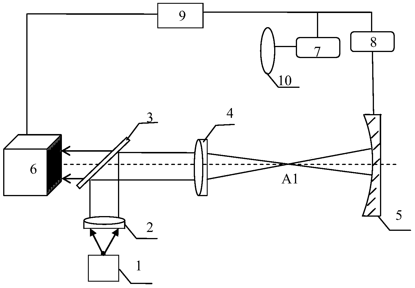
[0026] figure 1 Shown is the imaging wave aberration detection device of the objective lens imaging system. The light emitted by the light source 1 becomes parallel light after passing through the collimating mirror 2 , is reflected by the beam splitter 3 to the focusing mirror 4 , and converges to A1 on the focal plane of the focusing mirror 4 . That is, the light source 1 and the collimating mirror 2 constitute components for forming parallel light. The beam splitter 3 is used for splitting light from a parallel light source and transmitting reflected light with wave aberration information, and becomes an important component in the device. The focus...


PUM


Abstract

The invention discloses a wave aberration detection device of an objective lens imaging system. The wave aberration detection device comprises a light source, a collimating mirror, a spectroscope, a focusing mirror, a standard spherical reflector, a data processing unit, a wave-front sensor, a first accurate adjustment table and a second accurate adjustment table, wherein the collimating mirror, the spectroscope, the focusing mirror and the standard spherical reflector are sequentially placed in the light emitting direction of the light source, and the wave-front sensor, the first accurate adjustment table and the second accurate adjustment table are connected with the data processing unit. In the wave aberration detection device, the measurement processes and the system error calibration process are switched by changing the position of the standard spherical reflector 5; in the two measurement processes, the standard spherical reflector 5 has the same adjustment accuracy, and therefore the calibration, measurement and correction of device and system errors can be effectively completed, and the wave aberration measurement accuracy is improved. No high-precision standard light source is needed, and cost is reduced; A system error calibration method of the wave aberration detection device is simple and compact in structure and has the advantages of being easy to obtain and the like, and the wave aberration detection of the objective lens imaging system to be detected can be completed through the simple system.

Description

technical field [0001] The invention relates to the field of optical measurement technology, in particular to a wave aberration detection device for an objective lens imaging system and a correction method for the system error of the device, especially for wave images where the light source can be replaced and auxiliary optical devices can be added to the detection device as needed Differential measurement techniques. Background technique [0002] Waveform aberration measurement is often used in adaptive optics, optical inspection and evaluation and other fields. Especially in the adjustment of optical system and the evaluation of the imaging quality of objective lens, the measurement of wave aberration is an important means. [0003] The Hartmann sensor or shear interferometer is a widely used detection device for wave aberration. The traditional Hartmann wavefront sensor consists of microlens array, adapter lens, photodetector and data processing software. The incident ...

Claims


Application Information

Patent Timeline
Patent Type & Authority Applications(China)
IPC IPC(8): G01M11/02
Inventor 卢云君唐锋王向朝
Owner SHANGHAI INST OF OPTICS & FINE MECHANICS CHINESE ACAD OF SCI
Why Eureka
Try Eureka