Semiconductor memory device provided with error correcting code circuitry

a memory device and error correction technology, applied in the field of semiconductor memory devices, can solve the problems of inability to transmit information error inevitably in part of information bits, and inability to efficiently improve and correct pause refresh tail distribution, so as to reduce data holding current, reduce error rate, and efficiently correct bits

Active Publication Date: 2007-05-29
LONGITUDE LICENSING LTD
View PDF16 Cites 54 Cited by
  • Summary
  • Abstract
  • Description
  • Claims
  • Application Information

AI Technical Summary

Benefits of technology

[0013]In view of the above, it is an object of the present invention to provide a semiconductor memory device being capable of efficiently correcting bits having a low error rate in a Pause Refresh Tail distribution and of greatly reducing a data holding current by lengthening a refresh period so that the refresh period exceeds a period for a Pause Refresh real power.

Problems solved by technology

However, as such information consisting of multiple bits to be processed increases, an error occurs inevitably in part of bits of the information when being transmitted.
However, such the SDRAM as described above has a problem of a Pause Refresh Tail distribution of information to be stored in a memory cell, that is, a problem of a Pause Refresh failure.
There is a problem in that, since such the conventional semiconductor memory devices as described above cannot be applied to an SDRAM, when the Pause Refresh Tail distribution is to be improved and corrected, if bits have a low error rate, the Pause Refresh Tail distribution cannot be efficiently improved and corrected and therefore even by lengthening a refresh period so that the refresh period exceeds a period for the Pause Refresh real power, it is impossible to greatly reduce a data holding current.
Therefore, since the above pre-fetching operation is required, specifications for the SDRAM cannot be met.

Method used


Image

  • Semiconductor memory device provided with error correcting code circuitry
  • Semiconductor memory device provided with error correcting code circuitry
  • Semiconductor memory device provided with error correcting code circuitry

Examples


first embodiment

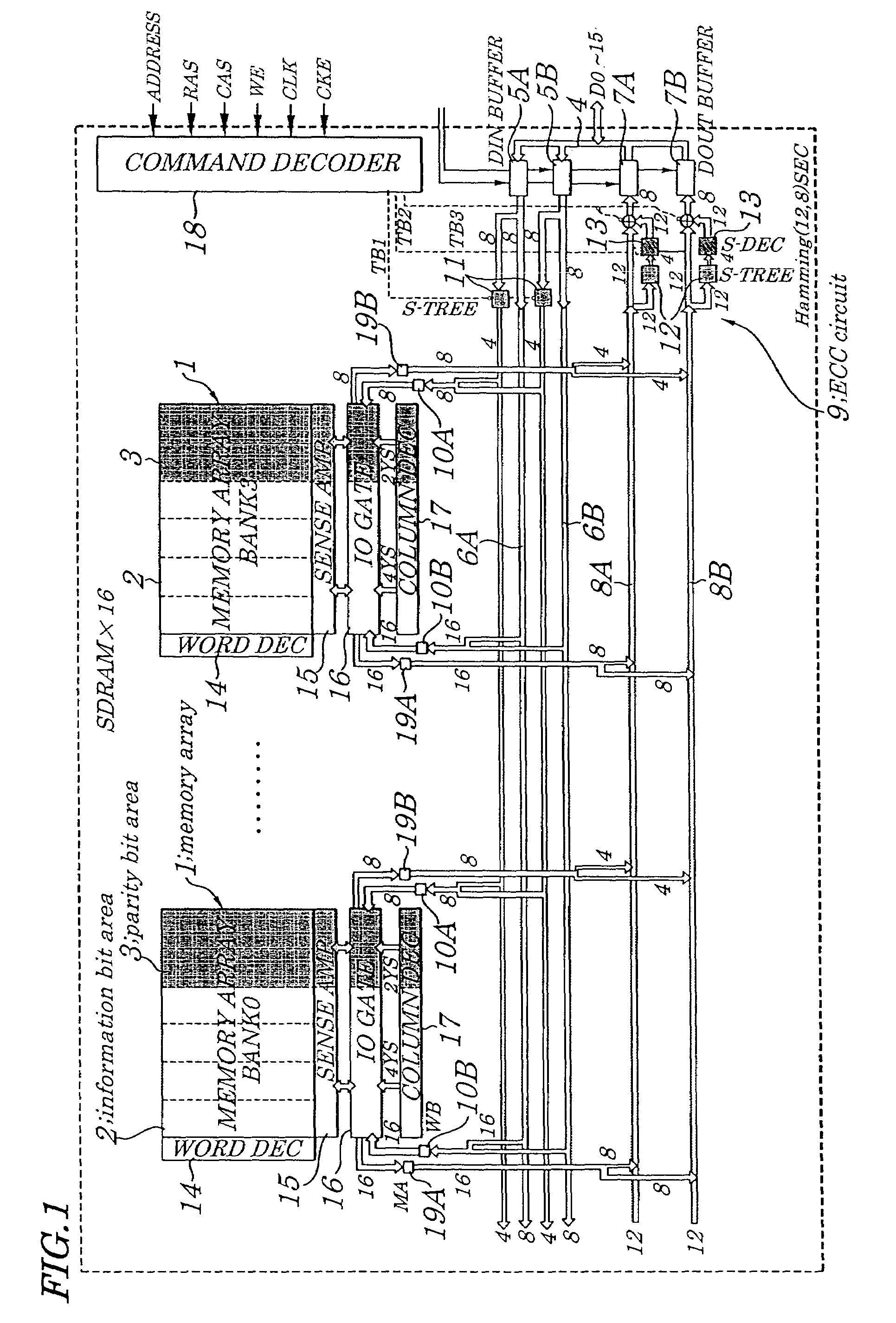
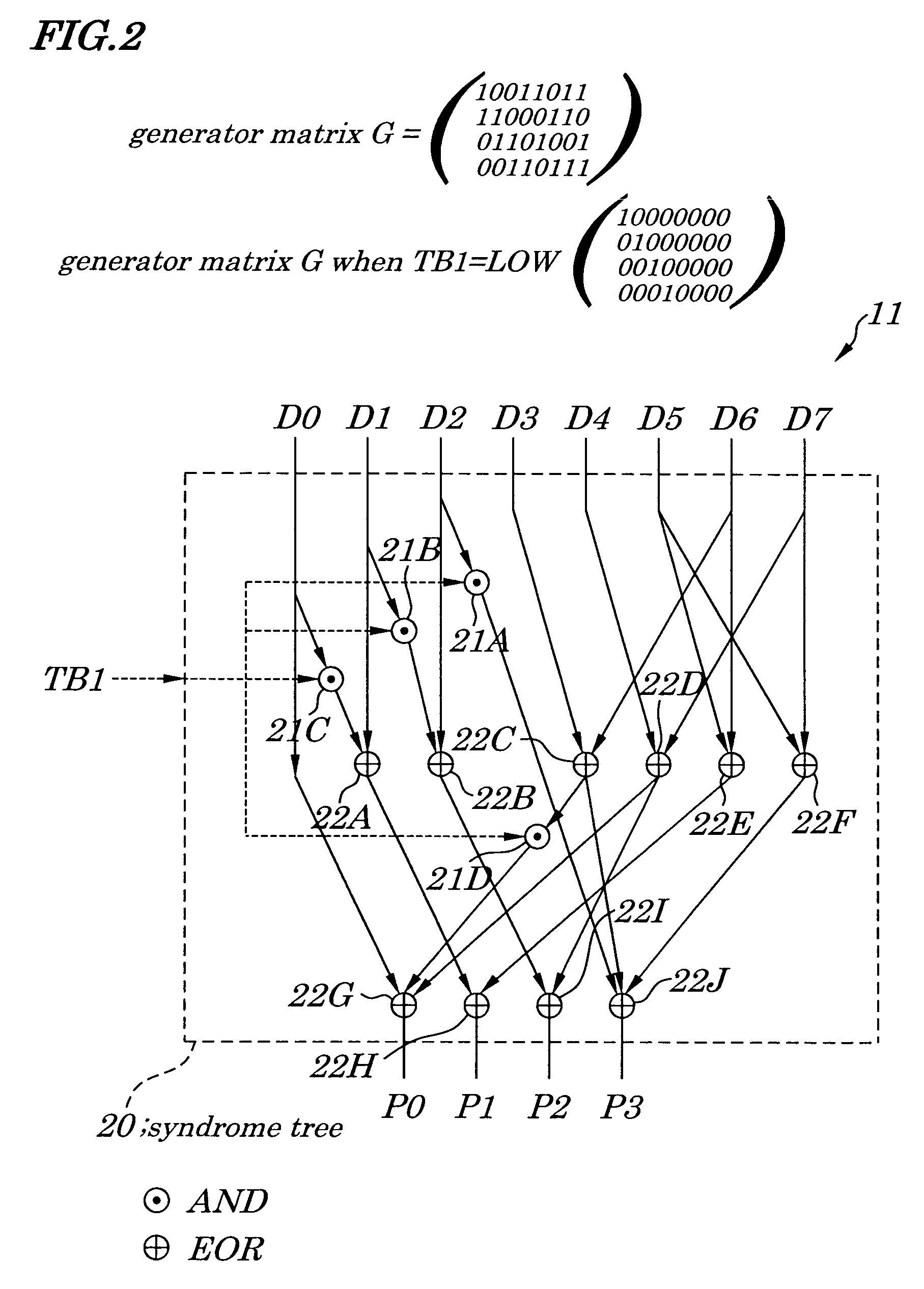
[0053]FIG. 1 is a schematic block diagram showing configurations of a semiconductor memory device according to a first embodiment of the present invention. FIG. 2 is a diagram for showing configuration of an encoding circuit 11 of the semiconductor memory device according to the first embodiment, FIG. 3 is a diagram for showing configuration of a decoding circuit 12 of the same semiconductor memory device, and FIG. 4 is a diagram for showing configuration of an error correcting circuit 13 of the same semiconductor memory device. Configurations of the semiconductor memory device of the first embodiment are described by referring to FIG. 1 to FIG. 4. The semiconductor memory device of the first embodiment, as shown in FIG. 1, is made up of a 16-bit SDRAM having a Hamming Code (12, 8)SEC, which includes memory arrays (MEMORY ARRAY) 1 made up of a plurality of memory cells and divided into four banks (first BANK0 to fourth BANK3) each containing an information bit area 2 and a parity bi...

second embodiment

[0071]FIG. 5 is a diagram for showing configurations of a semiconductor memory device according to a second embodiment of the present invention. FIG. 6 is a diagram showing configurations of an encoding circuit 11 of the semiconductor memory device according to the second embodiment. FIG. 7 is a diagram showing configurations of a decoding circuit 12 of the semiconductor memory device according to the second embodiment. Configurations of the semiconductor memory device of the second embodiment differ greatly from those of the semiconductor memory device of the first embodiment in that, in a 16-bit SDRAM having a Hamming Code (12, 8) SEC, use of a test signal is made unnecessary and output bus lines to output information bits read from a memory array are separated from output bus lines to output parity bits read from the memory array. In the semiconductor memory device of the second embodiment, as shown in FIG. 5, output bus lines 31A and 31B to divide 16 bits of information bits rea...

third embodiment

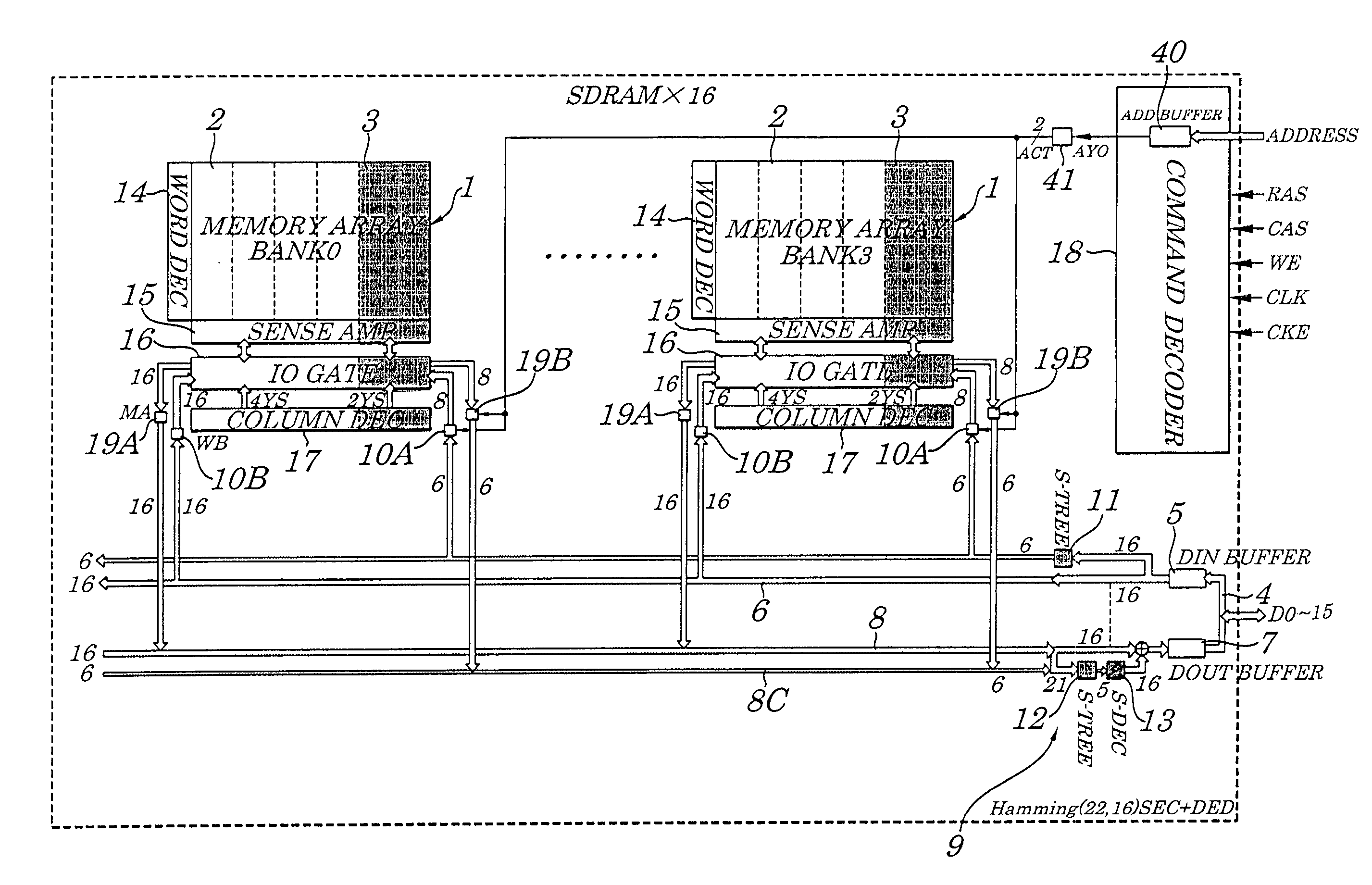
[0077]FIG. 8 is a diagram showing configurations of a semiconductor memory device according to a third embodiment of the present invention. Configurations of the semiconductor memory device of the third embodiment differ greatly from those of the above first embodiment in that a 16-bit SDRAM has a Hamming Code (21, 16).

[0078]The semiconductor memory device of the third embodiment, as shown in FIG. 8, includes an input bus line 6 to input 16 bits of information bits which are input and output through an input / output data bus 4 through an input buffer 5, an output bus line 8 to output 16 bits of information bits read from a memory array 1, an output bus line 8C to output 5 bits of parity bits read from the memory array 1, and an ECC circuit 9 placed on the input bus line 6 and output bus lines 8 and 8C. Moreover, the semiconductor memory device of the third embodiment is not so configured as to comply with specifications of DQM (Data Mask signal) and has an address controlling circuit...


PUM


Abstract

A semiconductor synchronous dynamic random access memory (SDRAM) device capable of correcting bits having a low error rate in a Pause Refresh Tail distribution and of reducing a data holding current by lengthening a refresh period so that the refresh period exceeds a period for a Pause Refresh real power. The semiconductor memory device is made up of a 16-bit SDRAM having a Hamming Code and including an ECC (Error Correcting Code) circuit made up of an encoding circuit controlled by a first test signal to output a parity bit corresponding to an information bit, a decoding circuit controlled by second test signal to output an error location detecting signal indicating an error bit in codeword, and an error correcting circuit controlled by a third test signal to input an error location detecting signal and to output an error bit in a reverse manner.

Description

BACKGROUND OF THE INVENTION[0001]1. Field of the Invention[0002]The present invention relates to a semiconductor memory device and more particularly to the semiconductor memory device being provided with an error correcting code (ECC) circuit.[0003]The present application claims priority of Japanese Patent Application No. 2002-203334 filed on Jul. 11, 2002, which is hereby incorporated by reference.[0004]2. Description of the Related Art[0005]A DRAM (Dynamic Random Access Memory) is employed in a storage section of various information devices such as personal computers and, as an amount of information increases, to process (that is, to write and read) information made up of multiple bits also increases. However, as such information consisting of multiple bits to be processed increases, an error occurs inevitably in part of bits of the information when being transmitted. To solve this problem, that is, to improve reliability in the transmission of the information, a DRAM with an ECC ...

Claims


Application Information

Patent Timeline
Patent Type & Authority Patents(United States)
IPC IPC(8): H03M13/00G11C29/42G06F11/10G11C11/401G11C11/406G11C29/04
CPCG06F11/1012G11C11/406G11C11/40615G11C2211/4062
Inventor ITO, YUTAKANAKAI, KIYOSHI
Owner LONGITUDE LICENSING LTD
Why Eureka
Try Eureka