Liquid crystal lens element and optical head device

a liquid crystal lens and optical head technology, applied in the field of liquid crystal lens element and optical head device, can solve the problems of deterioration of incident light convergence on information recording layer, writing error, and writing error, and achieve the effects of reducing the thickness of the liquid crystal layer, high speed response, and small siz

Inactive Publication Date: 2007-06-28
ASAHI GLASS CO LTD
View PDF11 Cites 53 Cited by
  • Summary
  • Abstract
  • Description
  • Claims
  • Application Information

AI Technical Summary

Benefits of technology

[0045] According to the present invention, a multi focal length variable liquid crystal lens capable of switching at least three types of transmission wavefront according to an applied voltage, can be realized. Moreover, since convex portions of the concave-convex portion having a cross-sectional shape of Fresnel lens or a Fresnel lens approximated by steps, are filled with a liquid crystal, it is possible to reduce the thickness of the liquid crystal layer, while generating a power component corresponding to a large optical path difference. Accordingly, such a construction leads to high speed response and it is possible to provide a liquid crystal lens element which has no moving part and can be small sized and which has a lens function stably correcting a spherical aberration containing a power component according to an applied voltage.
[0046] Further, by constructing an optical head device employing such a liquid crystal lens element, it is possible to efficiently correct a spherical aberration containing a power component generated due to the difference of cover thicknesses between single layer and double layer optical disks or due to variation of a cover thickness in an optical disk. Further, since there occurs little deterioration of aberration even in a case where the objective lens and the liquid crystal lens element are misaligned at a time of tracking, an optical head device capable of stably writing and / or reading, is realized.
[0047]FIG. 1: A vertical cross-sectional view showing the construction of a liquid crystal lens element of a first embodiment according to the present invention.
[0048]FIG. 2: A lateral cross-sectional view showing the construction of the liquid crystal lens element shown in FIG. 1.
[0049]FIG. 3: A graph showing the optical path difference of a transmission wavefront generated by the liquid crystal lens according to the first embodiment, wherein a is a graph showing the optical path difference by a unit of wavelength λ in relation to a radial position r shown in a horizontal axis. β is a graph showing an optical path difference of at least −λ and at most 0 obtained by subtracting an integer times of wavelength λ from α. γ is a graph showing an optical path difference plane-symmetrical to β about a plane of zero optical path difference.
[0050]FIG. 4: A side view showing an effect of switching applied voltage to the liquid crystal lens element of the first embodiment, wherein FIG. 4(A) shows a diverging transmission wavefront at an applied voltage V+1. FIG. 4(B) shows a transmission wavefront having no wavefront change at an applied voltage V0. FIG. 4(C) shows a converging transmission wavefront at an applied voltage V−1.

Problems solved by technology

In particular, in a case of double-layer DVD optical disk of writing type, deterioration of convergence causes decrease of converging power density, which causes a writing error, such being a problem.
In this case, if the cover thickness varies ±5 μm within the single layer BD optical disk, a large spherical aberration of about 50 mλ is generated in terms of RMS (Root Mean Square) wavefront aberration, which causes a problem that convergence of incident light on the information recording layer is deteriorated.
Further, in a case of double layer optical disk of recording type (hereinafter referred to as “double layer BD optical disk”) having cover thickness of 100 μm and 75 μm, a large spherical aberration generated according to the difference of the cover thickness, causes a writing error, such being a problem.
However, in the case of employing the movable lens group 160, there has been a problem that the size of the optical head device 100 becomes larger since the pair of lenses 161 and 162 and the actuator 163 are required, and the mechanical design for the movable lens becomes complicated.
Particularly, for writing and / or reading to / from a single layer or a double layer DVD optical disk or a BD optical disk, response within 1 second is required to correct a wavefront aberration generated due to variation of cover thickness or switching of recording layer type between a single layer type and a double layer type, which has been a problem.
Particularly, at a time of tracking operation in which the objective lens moves about ±0.3 mm in a radial direction of the optical disk, a large aberration due to the misalignment with the liquid crystal lens occurs, and there occurs a problem that convergence on the information recording layer is deteriorated to prevent writing and / or reading.
Accordingly, by employing an optical modulation element 300, it is possible to switch the focal point between two positions by switching presence and absence of the applied voltage, but switching of the focal point to a position between them has been difficult.
As a result, it has not been possible to reduce a spherical aberration in a case of cover thickness of from 0.56 mm to 0.63 mm required for a single layer and a double layer DVD optical disk, to be an RMS wavefront aberration level of at most 30 mλ.
Further, also in a case of a single layer or a double layer BD optical disk, it has not been possible to reduce a spherical aberration generated when the cover thickness varies ±5 μm, to an RMS wavefront aberration level of at most 50 mλ.
As a result, it has not been possible to solve a problem that a large spherical aberration generated due to the difference of cover thickness cannot be sufficiently corrected, which causes a writing error.

Method used


Image

  • Liquid crystal lens element and optical head device
  • Liquid crystal lens element and optical head device
  • Liquid crystal lens element and optical head device

Examples


first embodiment

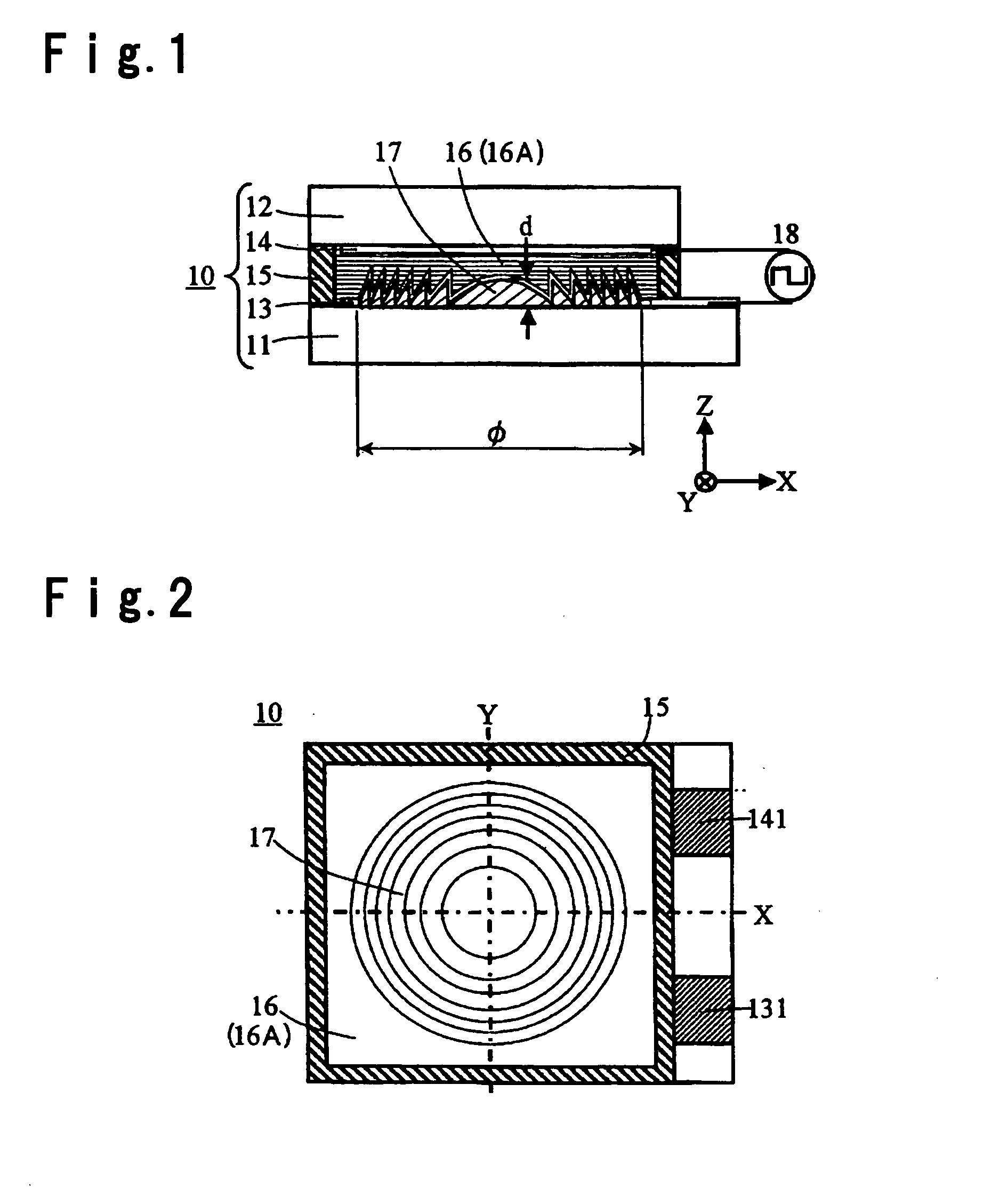
[0074] An example of the construction of the liquid crystal lens element 10 according to the first embodiment of the present invention, is described in detail with reference to a side view shown in FIG. 1 and a plan view shown in FIG. 2.

[0075] The liquid crystal lens element 10 of this embodiment comprises transparent substrates 11 and 12, transparent electrodes 13 and 14, a seal 15, a liquid crystal (liquid crystal layer) 16, a concave-convex portion 17 and an AC power source 18.

[0076] Among these, the concave-convex portion 17 has a shape of a Fresnel lens or a Fresnel lens approximated by steps, which is formed by employing a transparent material having a refractive index ns, and has a rotational symmetry about an optical axis (Z axis) of incident light within a region of effective diameter φ.

[0077] Then, an example of production process of the liquid crystal lens element 10, is described as follows.

[0078] First of all, on one of the flat surfaces (a top surface in FIG. 1) of...

second embodiment

[0118] An example of the construction of a liquid crystal lens element 20 according to the second embodiment of the present invention, is described in detail with reference to a side view shown in FIG. 5. Here, in this embodiment, same portions as those of the first embodiment are designated as the same reference numerals to avoid duplication of explanation.

[0119] The liquid crystal lens element 20 of this embodiment is different from the liquid crystal lens element 10 of the first embodiment in that the maximum depth d of a concave-convex portion 17B corresponds to the depth in a case of m=2 of the above-mentioned Formula (2). Accordingly, the distribution of the depth of the liquid crystal layer 16B is also different.

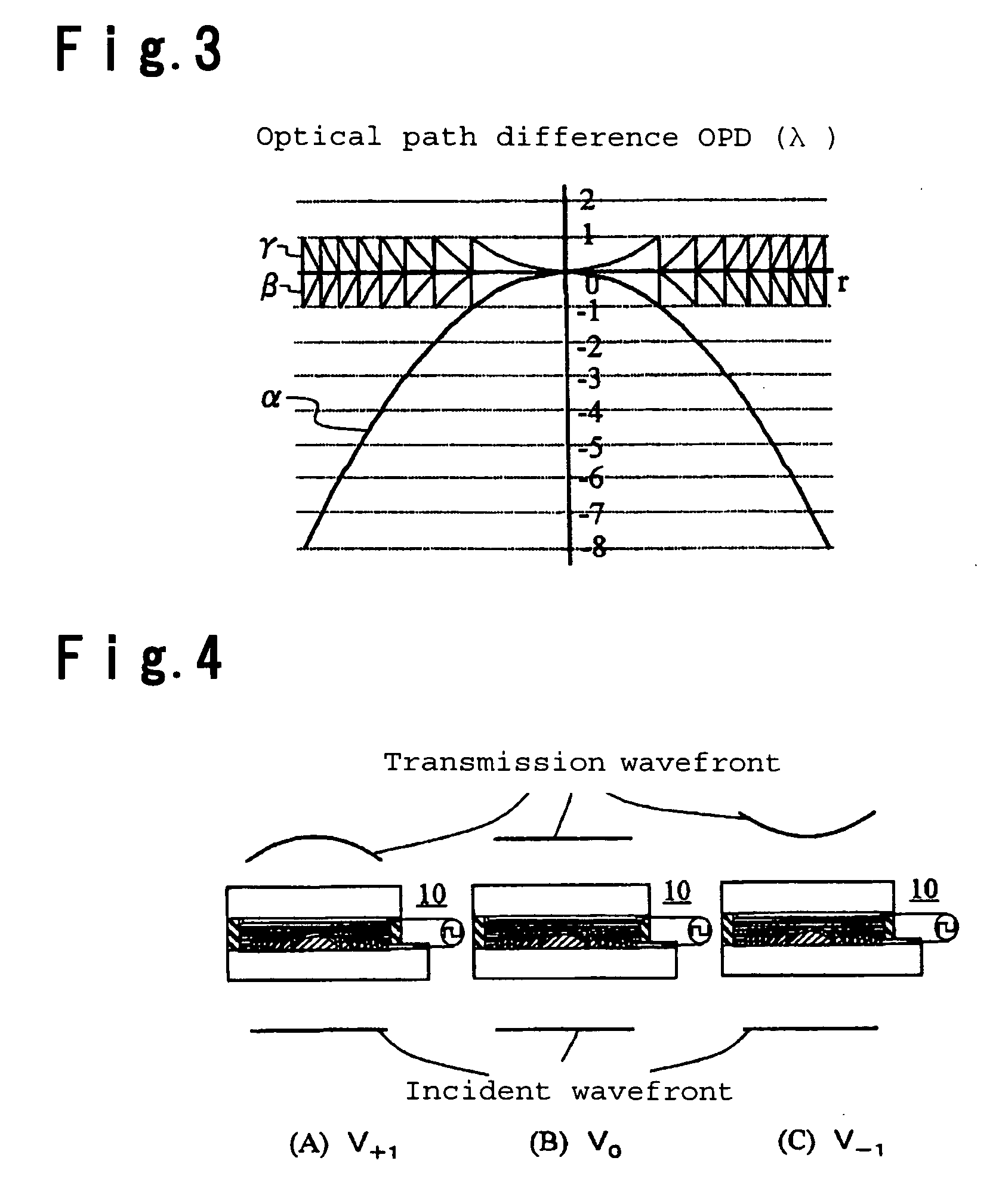
[0120] The concave-convex portion 17B of the liquid crystal lens element 20 according to this embodiment, is described as follows. Here, α of FIG. 6 is, in the same manner as α of FIG. 3, a graph showing an optical path difference OPD represented by Formula (3). Fur...

third embodiment

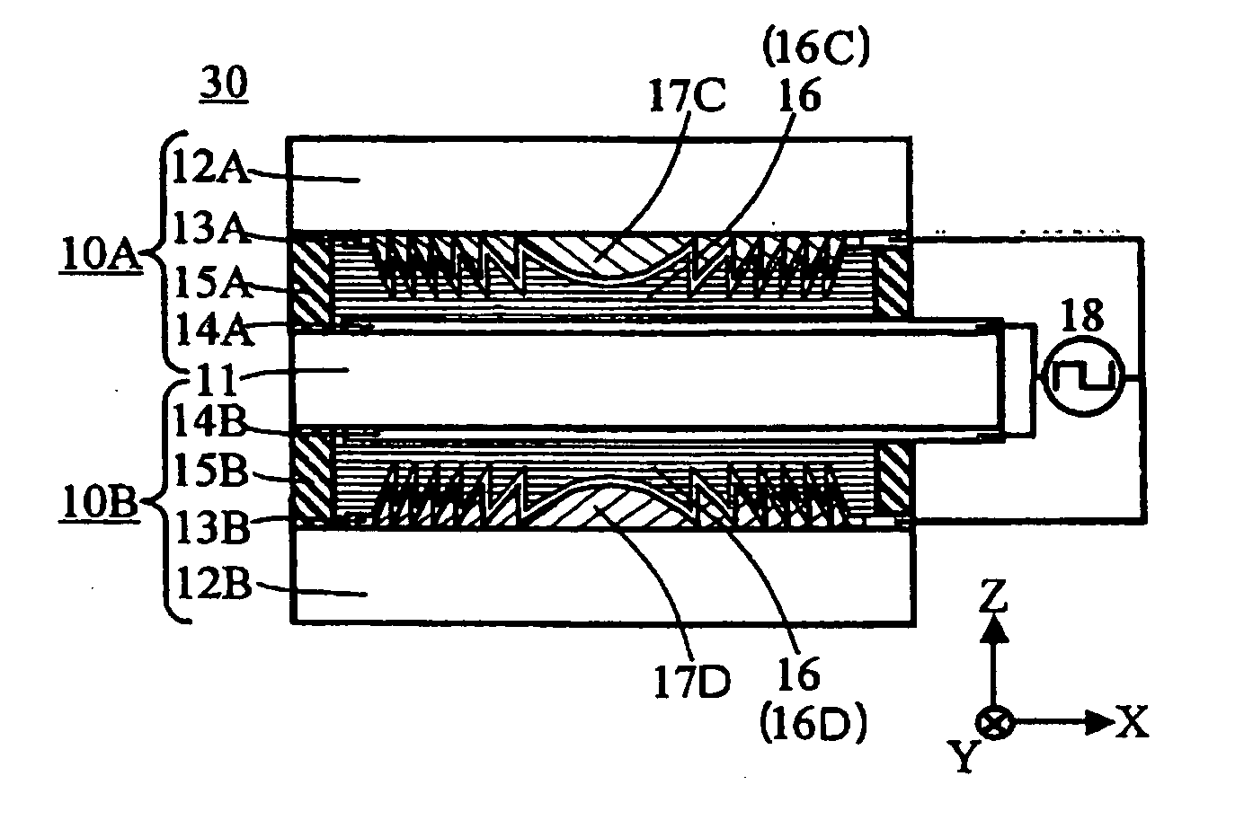
[0139] Then, the liquid crystal lens element 30 according to the third embodiment of the present invention, is described with reference to FIG. 8. Here, in this embodiment, portions common with those of the first embodiment, are designated by the same reference numerals to avoid duplication of explanation.

[0140] The liquid crystal lens element 30 of this embodiment comprises a first liquid crystal lens element 10A, a second lens element 10B and an AC power source 18 for applying AC voltage to these elements. The combination of the first and second liquid crystal lens elements 10A and 10B, has a construction that two liquid crystal lens elements 10 according to the first embodiment are laminated above and below so that their concave-convex portions 17 are opposed to each other (here, a transparent substrate 11 is shared).

[0141] Here, the first (the second) liquid crystal lens element 10A (10B) comprises a transparent substrate 11 on which a second transparent electrode 14A (14B) is...


PUM

PropertyMeasurementUnit
wavelength bandaaaaaaaaaa
thicknessaaaaaaaaaa
thicknessesaaaaaaaaaa

Abstract

A liquid crystal lens element is provided, which can realize a small sized element having no moving part, and which has a lens function of switching the focal length among multiple focal lengths of at least 3 types according to an applied voltage.
A liquid crystal lens element 10 is provided, which comprises a pair of transparent substrates 11 and 12 and a liquid crystal layer sandwiched between these substrates, wherein focal lengths of light transmitted through the liquid crystal 16 is changed depending on a voltage applied to the liquid crystal 16, the liquid crystal lens element 10 has a Fresnel lens-shaped concave-convex portion 17 and a liquid crystal layer 16A, and configured so that the refractive index n of the liquid crystal layer 16A changes from a refractive index n1 at a time of no application to a refractive index n2 at a time of voltage application, a refractive index ns of the concave-convex portion 17 is a value between the refractive indexes n1 and n2 and satisfies a predetermined relation, and the maximum depth d of the concave-convex portion 17 satisfies a predetermined relation, the focal length can be switched by switching an applied voltage to the liquid crystal layer 16A under the predetermined conditions.

Description

TECHNICAL FIELD [0001] The present invention relates to a liquid crystal lens element and an optical head device, in particular, to a liquid crystal lens capable of switching the focal length among a plurality of different focal lengths according to switching of applied voltage among a plurality of applied voltages, and an optical head device employing the liquid crystal lens, for writing and / or reading an information to / from an optical recording medium. BACKGROUND ART [0002] As examples of an optical recording medium (hereinafter referred to as “optical disk”) having an information recording layer formed on a surface of light-incident side, and a transparent resin covering the information recording layer, e.g. optical disks for CD and optical disks for DVD are widely used. Further, in an optical head device for writing and / or reading an information to / from the optical disks for DVD, e.g. a laser diode of 660 nm wavelength band as a light source and an objective lens having a NA (nu...

Claims


Application Information

Patent Timeline
Patent Type & Authority Applications(United States)
IPC IPC(8): G02F1/13G02B3/08G02B13/14G02F1/1333G02F1/29G11B7/00G11B7/135
CPCG02B3/08G02B13/14G02F1/133371G11B2007/13722G02F2001/294G11B7/1378G11B2007/0006G02F1/29G02F1/294G02F1/13G11B7/1372
Inventor OOI, YOSHIHARUTANABE, YUZURUSATO, HIROMASANOMURA, TAKUJISHIMIZU, RYUICHIRO
Owner ASAHI GLASS CO LTD
Why Eureka
Try Eureka