PMOS source and drain region ion implantation method and PMOS device manufacturing method

A device manufacturing method and ion implantation technology, which are used in semiconductor/solid-state device manufacturing, semiconductor devices, electrical components, etc., can solve the problems of PMOS reliability reduction, photoresist corrosion, etc., to reduce escape speed and improve reliability. , the effect of inhibiting corrosion phenomenon

Inactive Publication Date: 2014-12-24
SHANGHAI HUALI MICROELECTRONICS CORP
View PDF4 Cites 4 Cited by
  • Summary
  • Abstract
  • Description
  • Claims
  • Application Information

AI Technical Summary

Problems solved by technology

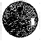
After the second step of fluorine injection, the product is scanned for surface defects, and it is often found that there are bubbles on the photore...

Method used


Image

  • PMOS source and drain region ion implantation method and PMOS device manufacturing method
  • PMOS source and drain region ion implantation method and PMOS device manufacturing method
  • PMOS source and drain region ion implantation method and PMOS device manufacturing method

Examples


Embodiment Construction

[0026] The specific implementation manner of the present invention will be described in more detail below with reference to schematic diagrams. Advantages and features of the present invention will be apparent from the following description and claims. It should be noted that all the drawings are in a very simplified form and use imprecise scales, and are only used to facilitate and clearly assist the purpose of illustrating the embodiments of the present invention.

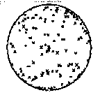
[0027] The inventor found that the reason for a large amount of fluorine precipitation is that both the boron difluoride implantation and the fluorine implantation contribute to the dose of fluorine, and if the total dose of fluorine is too large, it will exceed the solid solubility in the silicon substrate. When the silicon wafer is implanted, due to the existence of the self-heating effect, the fluorine element exceeding the solid solubility will escape from the silicon wafer substrate in the form of gas. The ...


PUM


Abstract

The invention provides a PMOS source and drain region ion implantation method and a PMOS device manufacturing method. The PMOS source and drain region ion implantation method comprises the steps that a substrate is provided, wherein a grid electrode structure is formed on the surface of the substrate, and side walls are formed on the two sides of the grid electrode structure; with the side walls serving as masks, PMOS source and drain region ion implantation is performed on the two sides of the grid electrode structure so that ions can be implanted into the substrate, wherein the implanted ions contain fluorine and boron difluoride, and the implantation of the fluorine and the boron difluoride is performed in the environment at the temperature ranging from -100 DEG C to -50 DEG C. The implantation of the fluorine and the boron difluoride is performed in the environment at the temperature ranging from -100 DEG C to -50 DEG C, and the environment at the temperature ranging from -100 DEG C to -50 DEG C can inhibit the temperature rise effect of silicon wafers during implantation of the fluorine and the boron difluoride; accordingly, the escape speed of the fluorine element can be lowered, and corrosion of photoresist is inhibited.

Description

technical field [0001] The invention relates to the field of semiconductor manufacturing, in particular to a PMOS source-drain region ion implantation method and a PMOS device manufacturing method. Background technique [0002] In the semiconductor manufacturing process, when implanting donor / acceptor elements, non-donor / acceptor elements are often used for co-implantation to achieve the required auxiliary effect. [0003] The most common auxiliary implant elements are germanium, silicon, carbon, fluorine, nitrogen and so on. The roles of various elements vary, for example, germanium and silicon are mainly used for pre-amorphization, carbon is mainly used for inhibiting diffusion, and fluorine is mainly used for improving negative bias temperature instability (NBTI) and suppressing short channel effects (SCE). [0004] When implanting the source and drain regions of PMOS, boron difluoride (BF2) and fluorine (F) are often used for co-implantation, because the introduction o...

Claims


Application Information

Patent Timeline
IPC IPC(8): H01L21/266H01L21/336
CPCH01L21/26506H01L21/266H01L29/66477
Inventor 邱裕明肖天金余德钦
Owner SHANGHAI HUALI MICROELECTRONICS CORP
Why Eureka
Try Eureka