

Method for manufacturing vertical SiGe FinFET
A fin and semiconductor technology, applied in the field of vertical SiGe FinFET fabrication, can solve performance and integration constraints and other issues
- Summary
- Abstract
- Description
- Claims
- Application Information
AI Technical Summary
Problems solved by technology
Method used
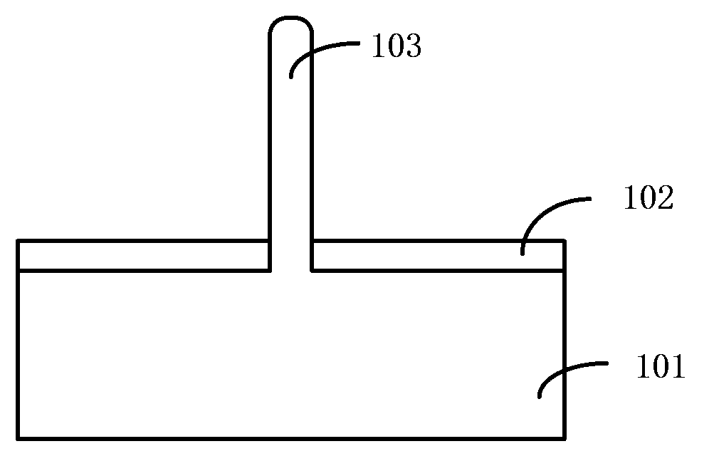
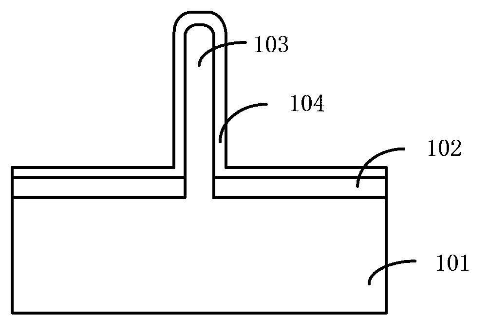
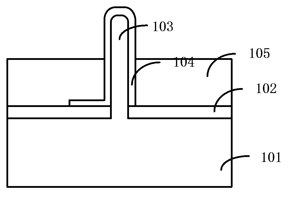
Image

Examples
Embodiment Construction
[0039] In the following description, numerous specific details are given in order to provide a more thorough understanding of the present invention. It will be apparent, however, to one skilled in the art that the present invention may be practiced without one or more of these details. In other examples, some technical features known in the art are not described in order to avoid confusion with the present invention.
[0040] In order to thoroughly understand the present invention, a detailed description will be provided in the following description to illustrate the method for fabricating the vertical SiGe FinFET of the present invention. Obviously, the practice of the invention is not limited to specific details familiar to those skilled in the semiconductor arts. Preferred embodiments of the present invention are described in detail below, however, the present invention may have other embodiments besides these detailed descriptions.
[0041] It should be noted that the te...
PUM
 Abstract
Description
Claims
Application Information