
SOI-LDMOS (silicon-on-insulator laterally diffused metal oxide semiconductor) high-tension power device with triangular trench

A technology of high-voltage power devices and triangular grooves, which is applied in semiconductor devices, electrical components, circuits, etc., can solve the problems of unfavorable low-voltage circuit integration, increase of on-resistance, and decrease of doping concentration, so as to alleviate the self-heating effect and improve the longitudinal endurance. The effect of pressure and equivalent thickness is thin

Inactive Publication Date: 2014-12-24
XIHUA UNIV
View PDF3 Cites 1 Cited by
  • Summary
  • Abstract
  • Description
  • Claims
  • Application Information

AI Technical Summary

Problems solved by technology

But SiO 2 It is a poor conductor of heat, increasing the thickness of the buried oxide layer will make the self-heating effect more serious, and increasing the thickness of the drift region will lead to a decrease in doping concentration, and a rapid increase in the specific on-resistance. Low voltage circuit integration

Method used


Image

  • SOI-LDMOS (silicon-on-insulator laterally diffused metal oxide semiconductor) high-tension power device with triangular trench
  • SOI-LDMOS (silicon-on-insulator laterally diffused metal oxide semiconductor) high-tension power device with triangular trench
  • SOI-LDMOS (silicon-on-insulator laterally diffused metal oxide semiconductor) high-tension power device with triangular trench

Examples


Embodiment Construction

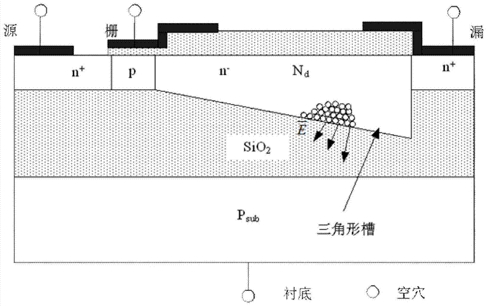
[0018] Such as figure 1 As shown, a SOI-LDMOS high-voltage power device with triangular grooves mainly includes: a substrate electrode, a P-type substrate vertically from bottom to top, a drift region, a source electrode, a drain electrode, a gate electrode, an insulating SiO 2 Layer (often referred to as buried oxide layer) and hole layer; wherein the lateral ends of the drift region are respectively formed n + source area and n + Drain area, in n + On the edge of the source region is a p-body region; a triangular groove is etched on the buried oxide layer, so that there is a slope of the buried oxide layer under the drift region, and the hole layer is on the buried oxide layer on the slope.

[0019] Wherein, the entire buried oxide layer is in the horizontal plane and can be completely integrated with the low-voltage circuit; therefore, when the buried oxide layer of this device is the same thickness as the conventional device, its equivalent thickness will be thinner tha...


PUM


Abstract

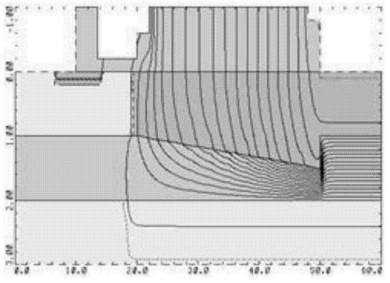
The invention discloses an SOI-LDMOS (silicon-on-insulator laterally diffused metal oxide semiconductor) high-tension power device with a triangular trench and aims to solve the problems that voltage of a drain of the prior SOI-LDMOS device is induced out of an electronic inversion layer from beneath a buried oxide layer, an equipotential line is prevented from penetrating the buried oxide layer, and early breakdown occurs to a silicon layer, and breakdown voltage withstanding is difficult to increase. The SOI-LDMOS high-tension power device is mainly characterized in that the triangular trench is etched in a buried oxide layer under a drift area; a buried oxide slope exists under the drift area and is capable of constraining positively charged holes, high-density positive charge is produced, and breakdown voltage withstanding of the device is greatly increased through the high-density positive charge; thickness of the drift area linearly increases from a source to a drain, according to the principle of RESURF (reduced surface field), a transverse electric field is uniformized owing to modulation, lateral voltage withstanding can be improved, and rejection ratio on resistance can be increased fast.

Description

technical field [0001] The invention belongs to the field of high-voltage power devices, in particular to an SOI-LDMOS high-voltage power device with triangular grooves. Background technique [0002] At present, when the SOI-LDMOS device is turned off in the existing technology, the drain voltage will induce an electron inversion layer under the buried oxide layer, which will prevent the equipotential line from passing through the buried oxide layer, causing breakdown to occur early in the silicon Layer, the problem that the longitudinal pressure resistance is difficult to improve. Because the improvement of the lateral withstand voltage can be achieved by increasing the length of the drift region and the lateral electric field, the improvement of the withstand voltage of SOI-LDMOS devices is mainly limited by the vertical withstand voltage. Theoretically speaking, increasing the thickness of the drift region and the buried oxide layer can improve the vertical withstand vol...

Claims


Application Information

Patent Timeline
Patent Type & Authority Applications(China)
IPC IPC(8): H01L29/78H01L29/06
CPCH01L29/7824H01L29/0634H01L29/66681
Inventor 阳小明李天倩卿朝进蔡育
Owner XIHUA UNIV
Learn More