Method for manufacturing multiple solder mask layers on PCB

A technology of solder mask and solder mask ink, which is applied in the manufacture of multi-layer circuits, application of non-metallic protective layers, secondary processing of printed circuits, etc. Low problems, to avoid scratches or pollution, easy operation, and improve production efficiency

Inactive Publication Date: 2014-12-24
SHENZHEN SUNTAK MULTILAYER PCB
View PDF3 Cites 2 Cited by
  • Summary
  • Abstract
  • Description
  • Claims
  • Application Information

AI Technical Summary

Problems solved by technology

[0003] The present invention aims at the problems that the existing multi-layer solder resist layer manufacturing method is prone to missing individual solder resist layers, which is inconvenient for inspection, and the inspection is prone to errors and omissions, and the inspection efficiency is low. It provides a method that can avoid missing individual solder resist layers. , and can be inspected directly and the manufacturing method of the multi-layer solder resist layer with high inspection efficiency

Method used


Image

  • Method for manufacturing multiple solder mask layers on PCB
  • Method for manufacturing multiple solder mask layers on PCB
  • Method for manufacturing multiple solder mask layers on PCB

Examples


Embodiment

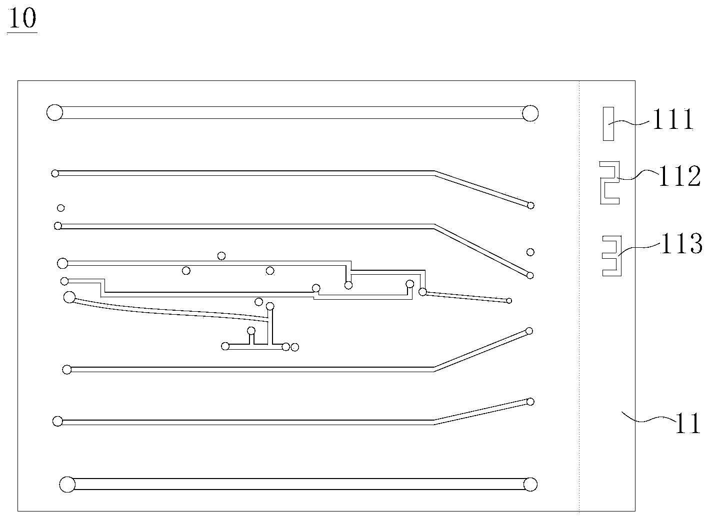
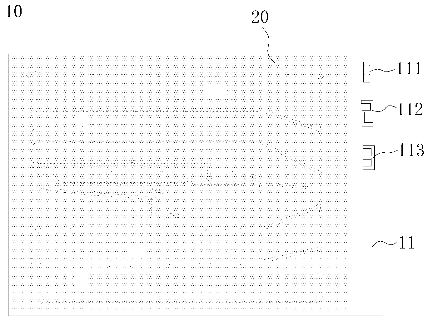
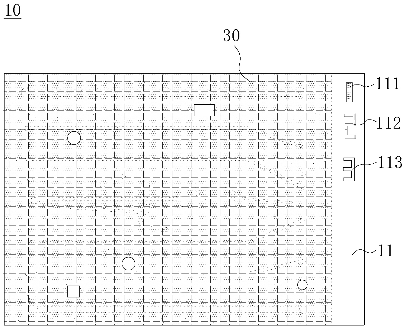
[0019] refer to Figure 1-4 , a kind of method for making three-layer solder resist layer on PCB provided by this embodiment, comprises the following steps:

[0020] (1) As in the circuit board production process of the prior art, the raw materials of each layer of circuit board are cut, and then the inner layer pattern transfer and pattern electroplating are carried out on each inner layer circuit board to form the inner layer circuit, and then each layer of circuit board is Lamination is carried out to form a multi-layer laminated board, and then holes are drilled on the multi-layer laminated board. After drilling, the multi-layer laminated board is subjected to copper sinking and full board electroplating. Then, make the outer layer graphics on the multilayer laminated board, and when making the outer layer graphics, design the logo (Arabic numerals) 111 for marking the three-layer solder resist layer that needs to be made later on the process side of the multilayer laminat...


PUM


Abstract

The invention relates to the technical field of production of PCBs, in particular to a method for manufacturing multiple solder mask layers on a PCB. The method includes the steps that first, identifications used for marking the solder mask layers are manufactured on a technological side, then, the solder mask layers are manufactured, the corresponding identifications are exposed at the same time, and the identifications are covered with the solder mask layers. According to the method, the identifications used for marking the solder mask layers are manufactured on the technological side of the PCB, the corresponding identifications are covered with the solder mask layer when each solder mask layer is manufactured, the corresponding identifications of the other solder mask layers which have not been manufactured are exposed, and therefore the manufacturing condition of the solder mask layers can be inspected through direct observation, inspection operation is easy and convenient to perform, and mistakes and omissions can be avoided; it is not needed that the PCB is moved to an magnifying lens device, and it can be avoided that the solder mask layers are scratched or contaminated in the moving process of the PCB. The method is simple and easy to implement and convenient to operate, and the production efficiency can be improved.

Description

technical field [0001] The invention relates to the technical field of PCB production, in particular to a method for manufacturing a multi-layer solder resist layer on a PCB. Background technique [0002] The printed circuit board is the support of electronic components and provides electrical connections for electronic components. The production process of printed circuit boards is generally: material cutting → inner layer pattern transfer → inner layer etching → lamination → drilling → sinking copper → full board electroplating → outer layer pattern transfer → pattern electroplating → etching → solder mask → surface Processing → forming processing. Among them, the solder resist layer is made on the PCB with the outer layer circuit, which can prevent short circuit and corrosion caused by moisture, chemicals, etc. between the conductor lines; it can also prevent open circuits caused by poor operation during the production and assembly of components; and It can insulate the...

Claims


Application Information

Patent Timeline
Patent Type & Authority Applications(China)
IPC IPC(8): H05K3/46H05K3/28
Inventor 林楠翟青霞姜雪飞姜翠红
Owner SHENZHEN SUNTAK MULTILAYER PCB
Why Eureka
Try Eureka