Centralized cache device and design method based on field programmable gate array

A design method and gate array technology, applied in computing, special data processing applications, instruments, etc., can solve problems such as increasing design costs, consuming FPGA hardware resources, and the design maximum frequency does not meet the requirements, so as to achieve less resource occupation and improve System clock frequency, effect of saving design cost

Active Publication Date: 2017-08-01
FENGHUO COMM SCI & TECH CO LTD
View PDF3 Cites 0 Cited by
  • Summary
  • Abstract
  • Description
  • Claims
  • Application Information

AI Technical Summary

Problems solved by technology

[0004] When the FPGA design contains N identical functional modules, the usual implementation method is to complete a functional module and then make N copies, such as figure 1 As shown, if a functional module occupies X combinational logic units, Y registers, and Z internal connections, then after N times of duplication, it will generally occupy X×N combinational logic units, Y×N registers, and Z×N There are only one internal connection, which seriously consumes the hardware resources of the FPGA and increases the design cost. At the same time, too many internal connections may also cause the maximum frequency (Fmax) that the entire design can achieve to fail to meet the requirements.

Method used


Image

  • Centralized cache device and design method based on field programmable gate array
  • Centralized cache device and design method based on field programmable gate array
  • Centralized cache device and design method based on field programmable gate array

Examples


Embodiment Construction

[0023] The present invention will be described in further detail below in conjunction with the accompanying drawings and embodiments.

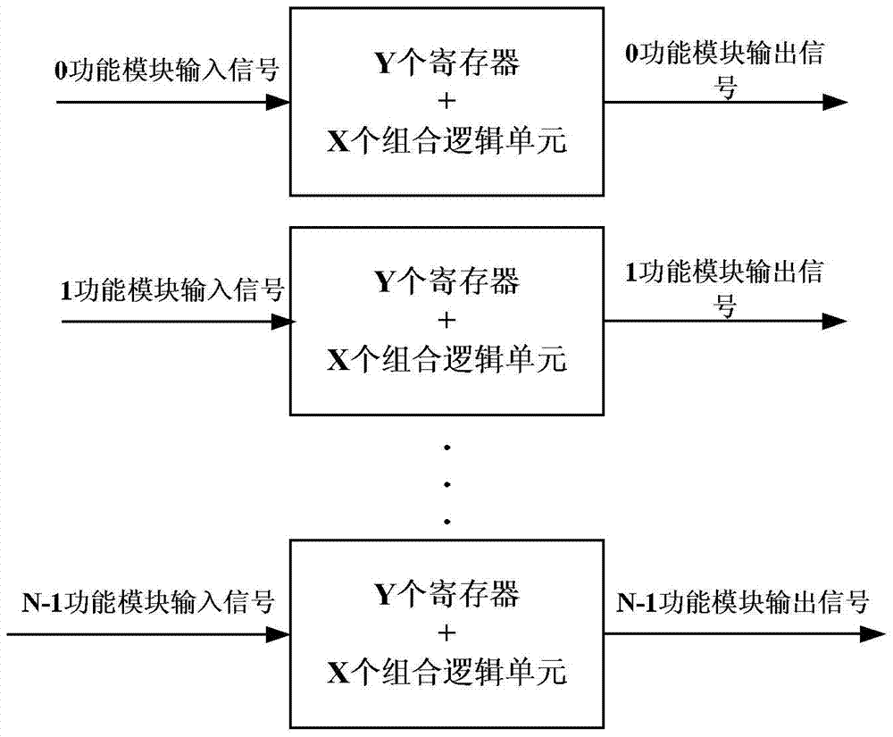
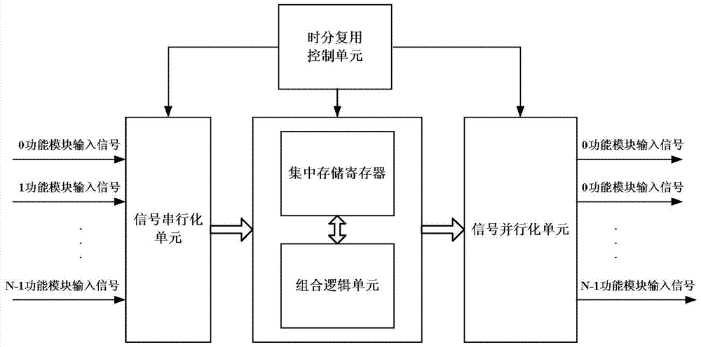
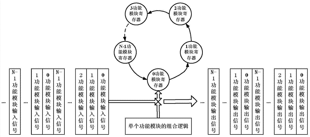
[0024] see figure 2 As shown, a centralized caching device based on a field programmable gate array is suitable for at least two identical functional modules, including a time division multiplexing control unit, a signal serialization unit, a centralized storage register, a combinational logic unit, and a signal parallelization unit. The time division multiplexing control unit is used to divide the time cycle into at least 2 time slots of equal duration, each time slot corresponds to a functional module in sequence, and each functional module performs input signal in the corresponding time slot Processing: the time slots divided by the time-division multiplexing control unit circulate continuously in sequence. The signal serialization unit is used to convert the parallel input signal of each functional module into a serial input signal; the ...


PUM


Abstract

The invention relates to a centralized-cache device and design method based on field-programmable gate arrays and relates to the field of field-programmable gate array design, and the centralized-cache device and design method is adaptive to at least two same functional modules. The device comprises a time division multiplexing control unit, a signal serialization unit, a centralizing storage register, a combinational logic unit and a signal parallelization unit. The time division multiplexing control unit is used for dividing the period into two time slots with the same length of time, each time slot corresponds to one functional module sequentially, and each functional module performs input signal processing in the corresponded time slot. The signal serialization unit is used for converting the parallel input signals of each functional module into serial input signals. The centralizing storage register is used for storing the register of each functional module and reading and writing the register of the functional module in the time slot corresponding to the functional module. The combinational logic unit is used for combinational logic of input signal processing of single functional module. The signal parallelization unit is used for restoring serial output signals as parallel output signals after the input signals of each functional module are processed.

Description

technical field [0001] The invention relates to the field of field programmable gate array design, in particular to a centralized cache device and design method based on field programmable gate array. Background technique [0002] FPGA (Field Programmable Gate Array, field programmable gate array) is in PAL (Programmable Array Logic, programmable array logic), GAL (Generic Array Logic, general array logic), PLD (Programmable Logic Device, programmable logic device), etc. The product of further development on the basis of programmable devices is the most integrated ASIC (Application Specific Integrated Circuit, application specific integrated circuit). The programmable feature of FPGA makes this device uniquely flexible, which can help system manufacturers launch products and realize industrialization in the shortest time; with the advancement of technology, the NRE (Non-Recurring Engineering, one-time Sexual engineering) costs are getting higher and higher, and traditional ...

Claims


Application Information

Patent Timeline
Patent Type & Authority Patents(China)
IPC IPC(8): G06F17/50
Inventor 程泉
Owner FENGHUO COMM SCI & TECH CO LTD
Why Eureka
Try Eureka