LED (light emitting diode) wafer encapsulation method
A chip packaging and chip technology, used in electrical components, circuits, semiconductor devices, etc., can solve the problems of low electrical conductivity and thermal conductivity, lack of ductility, and high cost, reducing thermal resistance, improving luminous efficiency, and reducing work. effect of temperature
- Summary
- Abstract
- Description
- Claims
- Application Information
AI Technical Summary
Problems solved by technology
Method used
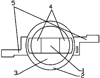
Image

Examples
Embodiment Construction
[0021] The specific implementation manner of the present invention will be further described.
[0022] A LED chip packaging method, the method comprises the following steps:
[0023] (1) Crystal expansion: Use an expansion machine to evenly expand the entire LED wafer film, so that the LED grains that are closely arranged on the surface of the film are pulled apart to facilitate spinning;
[0024] (2) Dot primer: Dot silver glue or insulating glue on the corresponding position of the bracket;
[0025] For GaAs and SiC conductive substrates, silver glue is used for red, yellow, and yellow-green chips with back electrodes; for blue and green LED chips with sapphire insulating substrates, insulating glue is used to fix the chips. Or use a glue preparation machine to apply silver glue on the back electrode of the LED product first, and then install the LED product with silver glue on the back of the LED product bracket. The efficiency of glue preparation is much higher than dispe...
PUM
 Abstract
Description
Claims
Application Information
 - Generate Ideas
- Intellectual Property
- Life Sciences
- Materials
- Tech Scout
- Unparalleled Data Quality
- Higher Quality Content
- 60% Fewer Hallucinations
Browse by: Latest US Patents, China's latest patents, Technical Efficacy Thesaurus, Application Domain, Technology Topic, Popular Technical Reports.
© 2025 PatSnap. All rights reserved.Legal|Privacy policy|Modern Slavery Act Transparency Statement|Sitemap|About US| Contact US: help@patsnap.com