Packaging shell based on LCP substrate and preparation method thereof

A technology for encapsulating shells and substrates, which is used in the manufacture of semiconductor/solid-state devices, electrical components, and electrical solid-state devices. Achieve the effect of light weight, better protection, and low dielectric loss

Active Publication Date: 2015-01-14
WUXI ZHONGWEI GAOKE ELECTRONICS
View PDF4 Cites 10 Cited by
  • Summary
  • Abstract
  • Description
  • Claims
  • Application Information

AI Technical Summary

Problems solved by technology

Its biggest shortcoming is that the water vapor permeability of ordinary PCB materials is poor, and it cannot be hermetically sealed, and the high temperature resistance of ordi

Method used


Image

  • Packaging shell based on LCP substrate and preparation method thereof
  • Packaging shell based on LCP substrate and preparation method thereof
  • Packaging shell based on LCP substrate and preparation method thereof

Examples


Embodiment Construction

[0035] The present invention will be further described below in conjunction with specific drawings and embodiments.

[0036] Such as figure 1 , Figure 2, image 3 Shown:

[0037] The present invention provides an LCP substrate packaging shell with a cavity structure. LCP, or Liquid Crystal Polymer, is a polymer with outstanding properties.

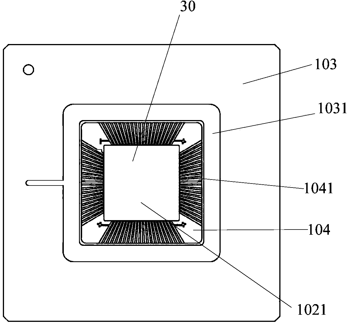
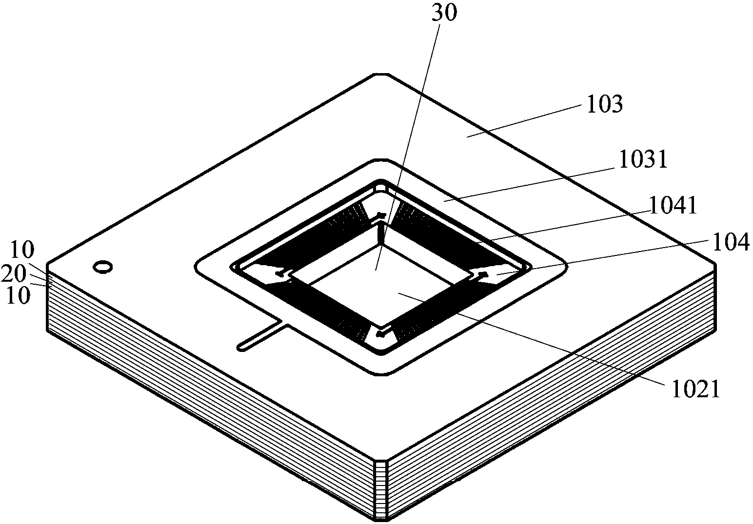
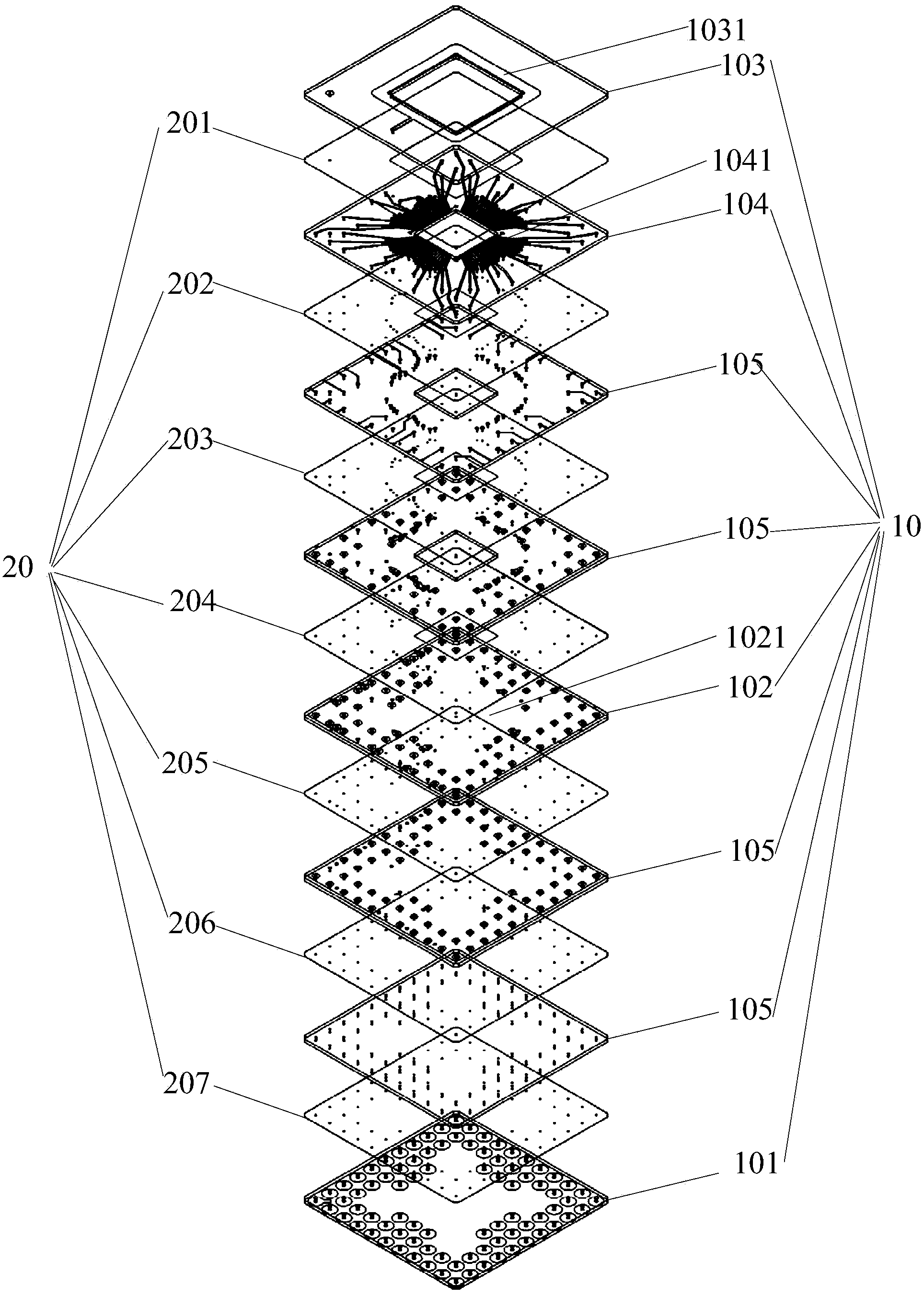
[0038] Such as Figure 1 ~ Figure 3 As shown, the package housing based on the LCP substrate includes a laminated structure formed by lamination of multiple LCP substrate composition layers 10; adjacent LCP substrate composition layers 10 are combined by each intermediate adhesive layer 20; wherein, each LCP substrate The composition layer 10 is made of an LCP single-layer copper-clad substrate. Each intermediate adhesive layer 20 is made of an LCP film substrate.

[0039] The LCP substrate composition layer 10 includes a bottom pad layer 101 located at the bottom of the laminate structure, a chip mounting layer 102 located in the middle of the...


PUM


Abstract

The invention provides a packaging shell based on an LCP substrate. The packaging shell comprises a lamination structure formed by laminating multiple LCP substrate composition layers; adjacent LCP substrate composition layers are combined through intermediate bonding layers; each LCP substrate composition layer comprises a bottom bonding pad layer located on the bottommost layer of the lamination structure, a chip mounting layer located in the middle of the lamination structure, a sealing layer located on the top layer of the lamination structure and a keying layer under the sealing layer; each LCP substrate composition layer further comprises at least one wiring interconnection layer arranged between the bottom bonding pad layer and the chip mounting layer and at least one wiring interconnection layer arranged between the keying layer and the chip mounting layer; all the layers of the lamination structure are electrically connected through via holes; each chip mounting layer is provided with a chip adhesion region, the positions, corresponding to the chip adhesion regions, of all the other layers above the chip mounting layers are provided with openings, and all the layers are stacked together to form a cavity used for containing a chip. The packaging shell has excellent high-frequency characteristics and air tightness.

Description

Technical field [0001] The invention belongs to the technical field of integrated circuit manufacturing, and relates to a plastic packaging cavity-type shell in high-density packaging, which is used for high-reliability packaging for high-frequency applications such as microwaves and millimeter waves, and specifically relates to a cavity structure , LCP package shell in the sealed area. Background technique [0002] At present, there are two main technical methods for high-density packaging of integrated circuits: one is a multilayer ceramic package with a cavity structure using high-temperature co-fired ceramic technology, and the other is a plastic that uses a multilayer PCB substrate as the chip substrate material. Package. Both adopt multilayer wiring technology, and both can achieve higher packaging density. Due to the use of different packaging dielectric materials and different process methods, the two have their own characteristics and their application fields are also ...

Claims


Application Information

Patent Timeline
IPC IPC(8): H01L23/043H01L23/06H01L21/50
Inventor 肖汉武
Owner WUXI ZHONGWEI GAOKE ELECTRONICS
Why Eureka
Try Eureka