A Method for Measuring the Shape of Freeform Surface

A surface and curved surface technology, which is applied to measuring devices, instruments, optical devices, etc., to achieve the effect of improving the measurement resolution

Active Publication Date: 2016-09-28
HARBIN INST OF TECH
View PDF7 Cites 0 Cited by
  • Summary
  • Abstract
  • Description
  • Claims
  • Application Information

AI Technical Summary

Problems solved by technology

[0003] In order to solve the above problems, the present invention discloses a device and method for measuring the surface shape of a free-form surface, which solves the problem of high-precision measurement of the surface topography of a free-form surface sample

Method used


Image

  • A Method for Measuring the Shape of Freeform Surface
  • A Method for Measuring the Shape of Freeform Surface

Examples


specific Embodiment 1

[0028] This embodiment is a device embodiment.

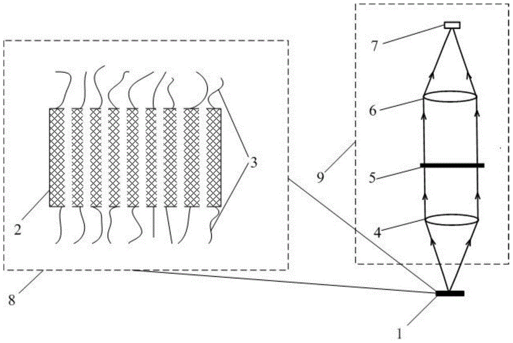
[0029] A device for measuring the shape of a free-form surface in this embodiment, the structural diagram is as follows figure 1 shown. The unit includes:

[0030] Electroluminescent film lighting part 8 and optical imaging measurement part 9;

[0031] The electroluminescent film lighting part is composed of a sample to be tested 1, an electroluminescent film 2 plated on the surface of the sample 1, and positive and negative microelectrodes 3;

[0032] The optical imaging part includes objective lens 4, optical filter 5, tube lens 6 and CCD7 in sequence along the propagation direction of the collected optical signal.

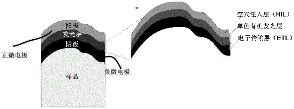
[0033] The above-mentioned device for measuring the shape of a free-form surface, the electroluminescent film as figure 2 As shown, its thickness is not more than 4 μm, and it is composed of a cathode layer, a light-emitting layer and a transparent anode layer, and the thickness of each layer is uniform; the ...

specific Embodiment 2

[0034] This embodiment is an embodiment of the method implemented on the device described in the first specific embodiment.

[0035] A kind of method for measuring free-form surface profile of the present embodiment, comprises the following steps:

[0036] In the first step, a cathode layer, a light-emitting layer, a transparent anode layer and a microelectrode with a total thickness of no more than 4 μm are formed on the surface of the sample 1, and the thickness of each layer is uniform; the film thickness of the light-emitting layer is no more than 1 μm, and the light-emitting layer is an organic layer. It is composed of an electron transport layer, a monochromatic organic light-emitting layer and a hole injection layer. The electroluminescent film is made in different regions and arranged in strips on the surface of sample 1. There are small blank areas without coating between different strips, and the blank areas are The width is less than 5nm, and there are positive and ...

specific Embodiment 3

[0045] This embodiment is a method embodiment.

[0046]In this embodiment, on the basis of the specific embodiment 2, an eleventh step is added to clean all the films on the surface of the sample 1 and the microelectrodes near the surface of the sample 1. In this step, the recovery of the surface topography of the sample can be realized.


PUM


Abstract

The invention provides a device and method for measuring a free-form surface type and belongs to the field of optical microscopic imaging. The device comprises a sample to be measured, an electroluminescent film plated on the surface of the sample, positive and negative microelectrodes, an objective lens, an optical filter, a tube lens, a CCD, an electroluminescent film illumination portion and an optical imaging measurement portion. According to the method, the electroluminescent fluorescent dielectric film is plated on the surface of the sample, the surface of the sample is illuminated after energization, the free-form surface type can be measured in combination with an optical detection optical path, odd stripes and even stripes of the surface of the sample are illuminated through electroluminescence to replace traditional optical illumination, the problem that the part with large curvature is unmeasured because of illumination apertures is solved, and the surface appearance of the sample in an area with a large included angle between a normal and the axial direction can be measured.

Description

technical field [0001] A device and method for measuring the surface shape of a free-form surface belong to the field of optical microscopic imaging. Background technique [0002] In the field of surface topography measurement and microscopic imaging, the measurement of optical free-form surfaces has always been a very challenging problem. Common optical measuring instruments, such as confocal microscopes, illuminate the surface of the sample by projecting light onto the sample through structures such as lenses. However, the traditional optical illumination mode cannot fully illuminate the area where the sample surface normal and the optical axis have an inclination angle of more than 45 degrees and effectively collect the sample surface signal light. Contents of the invention [0003] In order to solve the above problems, the present invention discloses a device and method for measuring the surface profile of a free-form surface, which solves the problem of high-precisio...

Claims


Application Information

Patent Timeline
Patent Type & Authority Patents(China)
IPC IPC(8): G01B11/24
Inventor 刘俭谭久彬王红婷
Owner HARBIN INST OF TECH
Why Eureka
Try Eureka