Device equivalent circuit model parameter extracting method and bonding pad parasitic parameter extracting method

An equivalent circuit model and parameter extraction technology, which is applied in electrical digital data processing, instruments, and special data processing applications, etc., can solve problems such as the difficulty of completely stripping parasitic capacitance parameters and affecting the accuracy of extracted inductance.

Active Publication Date: 2015-01-21
SOUTHEAST UNIV
View PDF5 Cites 16 Cited by
  • Summary
  • Abstract
  • Description
  • Claims
  • Application Information

AI Technical Summary

Problems solved by technology

However, there are certain defects in this method. Because the parasitic capacitance parameters are difficult to completely peel off, when the curve of the real part of the Z parameter and the frequency is drawn to extract the parasitic resistance parameter, the curve of the real part of the Z parameter and the resistance will appear to be dependent on frequency. At the same time, it will also affect the accuracy of extracting the inductance from the imaginary part of the Z parameter (Gu D, Wallis T M, Blanchard P, et al. De-embedding parasitic elements of GaN nanowire metal semiconductor field effect transistors by use of microwave measurements[J]. Applied Physics Letters, 2011, 98(22): 223109. Reference 4)
There will be a large error

Method used


Image

  • Device equivalent circuit model parameter extracting method and bonding pad parasitic parameter extracting method
  • Device equivalent circuit model parameter extracting method and bonding pad parasitic parameter extracting method
  • Device equivalent circuit model parameter extracting method and bonding pad parasitic parameter extracting method

Examples


Embodiment Construction

[0034] The present invention will be further described below in conjunction with the accompanying drawings and specific embodiments.

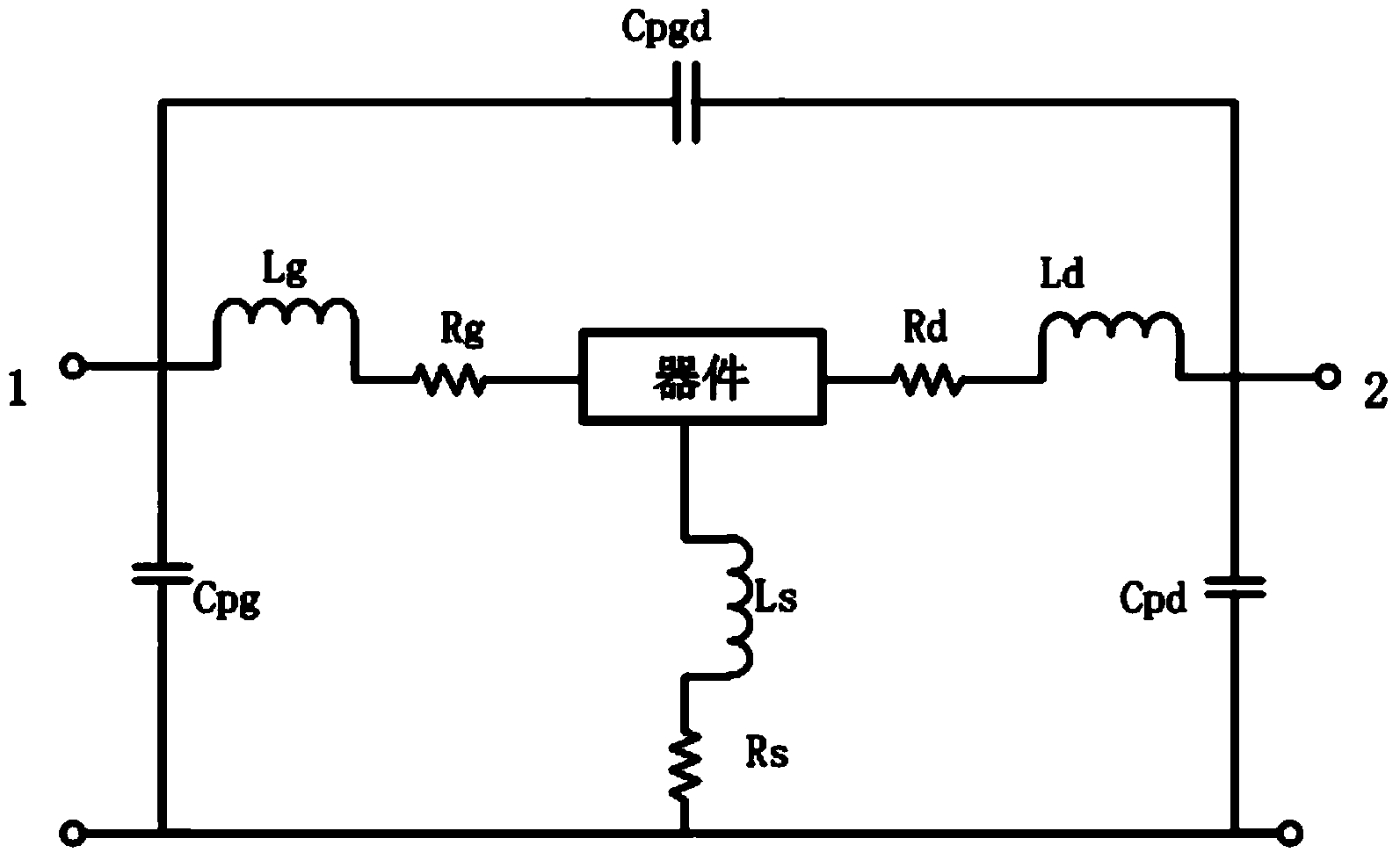
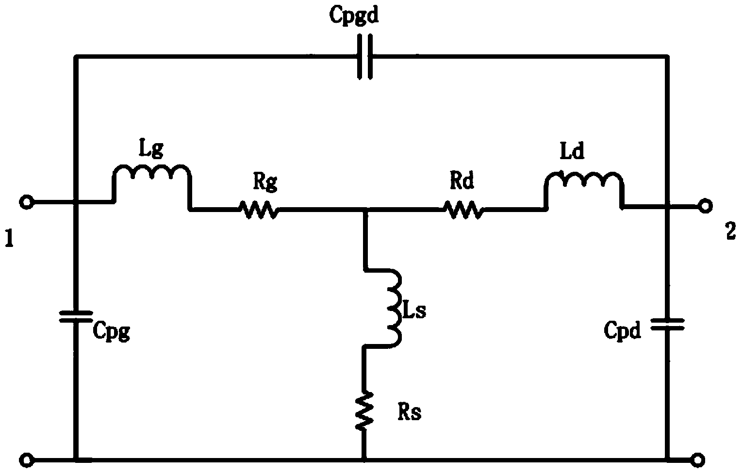
[0035] figure 1 It is the device test equivalent circuit diagram used in the method for extracting pad parasitic parameters in the embodiment of the present invention, and the equivalent circuit diagram includes the peripheral parasitic capacitance C pg 、C pd 、C pgd , the series parasitic resistance R g , R d , R s and series series parasitic inductance L g , L d , L s . The method of parameter extraction here is also an illustration of how to extract the above parameters in this equivalent circuit diagram.

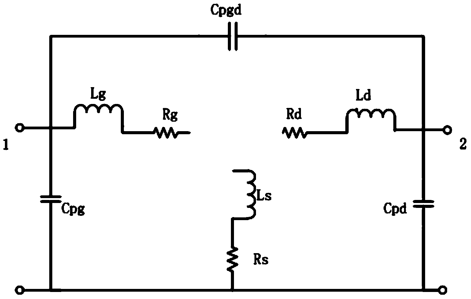
[0036] figure 2 It is the topology diagram of the equivalent circuit model under the pad open circuit structure in which the peripheral parasitic capacitance parameters are extracted in the pad parasitic parameter extraction method of the embodiment of the present invention, including three peripheral parasitic capacitance param...


PUM


Abstract

The invention discloses a device equivalent circuit model parameter extracting method and mainly aims at solving the problems in the prior art, such as complicated extracting process and inaccurate extracting results. The parasitic parameter extracting method comprises the following steps: dividing a short-circuit bonding pad equivalent circuit from which a parasitic capacitor is de-embedded into independent networks for further analysis, and synchronously extracting parasitic resistance and parasitic inductance parameters. The invention further discloses a bonding pad parasitic parameter extracting method applying the equivalent circuit parameter extracting method. Simulation results show that parasitic parameter extracting results are highly matched with scattering parameters of actual device test results, and the parameters are more accurately and rapidly extracted.

Description

technical field [0001] The invention relates to a device equivalent circuit model parameter extraction method and a de-embedded transistor device test pad parasitic parameter extraction method, belonging to the technical field of integrated circuits. Background technique [0002] Transistor models mainly include two types, physical models and equivalent circuit models. Among them, the equivalent circuit model is a general and effective model for simulating transistors. Establishing an accurate equivalent circuit model is the key to the success of circuit design. The core factor that reduces the cost of development and production. [0003] For the transistor device model, the calibration of test equipment, de-embedding of pad parasitics, the topology of the equivalent circuit and the extraction method of parameters will all affect the accuracy of the model (Erickson N, Shringarpure K, Fan J, et al. De-embedding Techniques for transmission lines: An exploration, review, and ...

Claims


Application Information

Patent Timeline
Patent Type & Authority Applications(China)
IPC IPC(8): G06F17/50
Inventor 唐旭升黄风义张有明李剑宏杨江
Owner SOUTHEAST UNIV
Why Eureka
Try Eureka