Supercharge Your Innovation With Domain-Expert AI Agents!

Negative pressure converting circuit

A negative pressure conversion and circuit technology, applied in information storage, static memory, instruments, etc., can solve the problems of not reaching the minimum value, not reaching the maximum value, and failing to meet the frequency requirements, so as to improve the working speed and change speed, effect of avoiding adverse effects

Active Publication Date: 2015-01-21
SHANGHAI HUAHONG GRACE SEMICON MFG CORP
View PDF4 Cites 4 Cited by
  • Summary
  • Abstract
  • Description
  • Claims
  • Application Information

AI Technical Summary

Problems solved by technology

[0004] When the input signal vin changes from high to low, the signal vinb changes from low to high, assuming that the positive power supply voltage is 1.0V and the negative power supply voltage is -6V, the absolute values ​​of the threshold voltages of PMOS transistors MP101 and 102 and NMOS transistors MN101 and 102 are the same , that is, Vtp=Vtn=0.7, then the PMOS transistor MP102 is in the state of saturation, and its overdrive voltage is only 0.3V, which causes the current in the branch of the PMOS transistor MP102 to be too small, the output signal Voutb rises slowly, and Vout falls slowly, which cannot meet the frequency Requirements, in order to achieve the frequency characteristics as much as possible, the width-to-length ratio of the PMOS tube and the NMOS tube is usually different by tens or even hundreds of times, but the too large size of the MOS tube affects the speed of the voltage conversion circuit
like figure 2 Shown is the simulation waveform of the input and output of the existing negative voltage conversion circuit; the positive power supply is 1V, the frequency of the input signal vin is 50MHz, the curve 102 corresponds to the simulation curve of the output signal Vout, and the curve 103 corresponds to the simulation of the output signal Voutb It can be seen from the curve that when the input signal Vin is converted from high level to low level, the output signal Voutb rises slowly and cannot reach the required maximum value, and the output signal Vout decreases slowly and cannot reach the required minimum value. , so the existing negative voltage conversion circuit cannot realize the demand for high-speed conversion of low power supply voltage

Method used


Image

  • Negative pressure converting circuit
  • Negative pressure converting circuit
  • Negative pressure converting circuit

Examples


Embodiment Construction

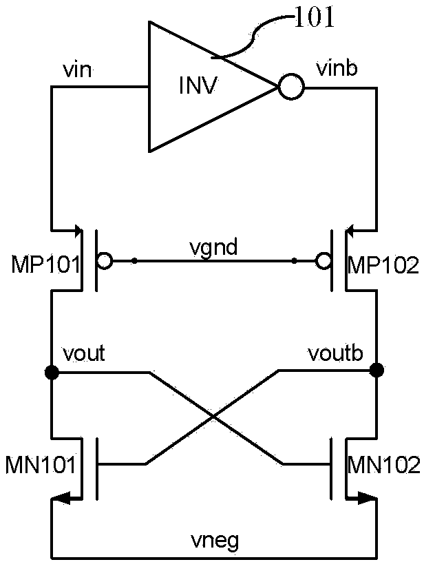
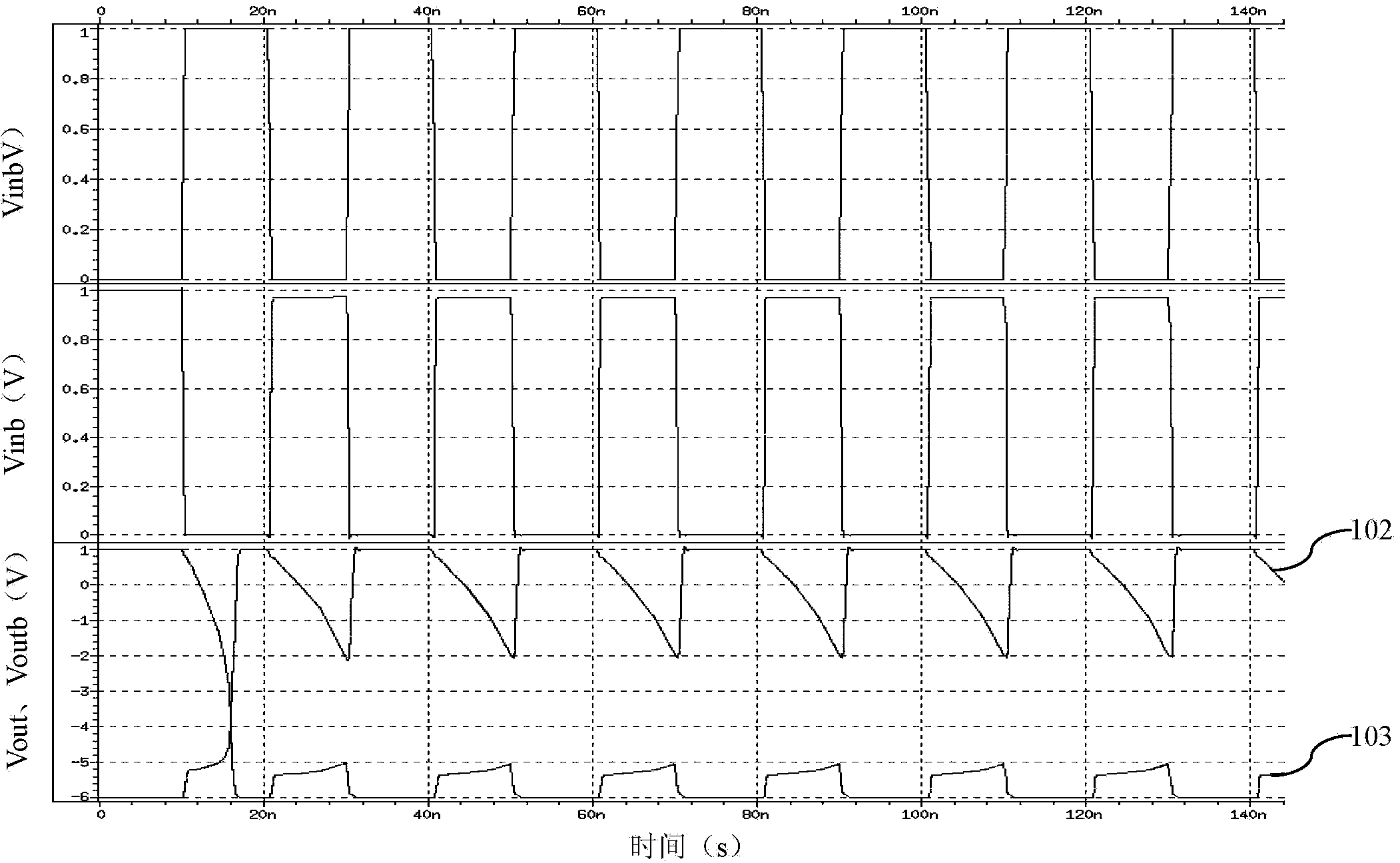
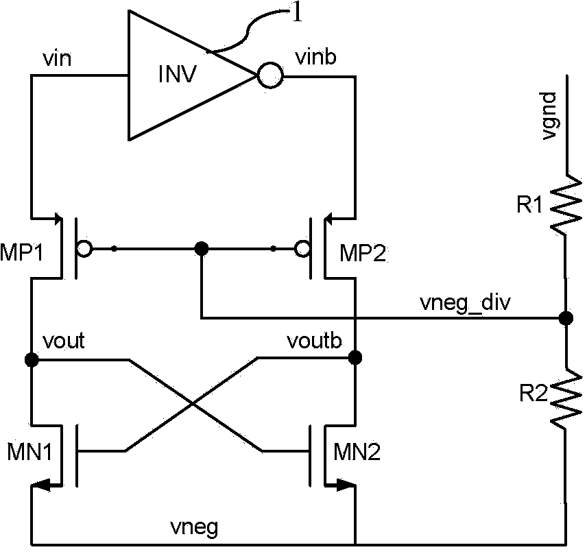
[0023] like image 3 Shown is the negative voltage conversion circuit diagram of the embodiment of the present invention; the negative voltage conversion circuit of the embodiment of the present invention is used to convert positive logic level signals into negative logic level signals, including: an inverter 1, a first PMOS transistor MP1, The second PMOS transistor MP2, the first NMOS transistor MN1, the second NMOS transistor MN2, and a resistor are connected in series.

[0024] The input terminal of the inverter 1 is connected to the input signal vin, and the output terminal outputs the inverted signal vinb of the input signal vin, the operating power supply of the inverter 1 is a positive power supply, and the input signal vin is a positive logic voltage. A flat signal, the high level of the input signal vin is the same as the positive power supply, the low level of the input signal vin is smaller than the high level, and the low level of the input signal vin is greater t...


PUM


Abstract

The invention discloses a negative pressure converting circuit, including an inverter, a first PMOS tube, a second PMOS tube, a first NMOS tube, a second NMOS tube and a resistor series circuit. An inverter inverts an input signal, source electrodes of the two PMOS tubes are respectively connected into the input signal and the inverted signal, drain electrodes of the two PMOS tubes respectively output two mutually inverted output signals, drain electrodes of the two NMOS are respectively connected with an output signal and are intersected the grid of the other NMOS tube, source electrodes of the two NMOS tubes are connected to a negative supply, the resistor series circuit is in series connection between the ground and the negative supply and provides a differential pressure signal to the two grids of the two PMOS tubes. The invention can realize high speed working under low supply voltage.

Description

technical field [0001] The invention relates to a semiconductor integrated circuit, in particular to a negative voltage conversion circuit. Background technique [0002] Negative voltage circuits are widely used in electrical erasable programmable read-only memory (EEPROM), flash memory (Flash) and other circuits. The data signal in the negative voltage circuit samples negative logic level signals, and the high voltage of negative logic level signals Negative voltages appear in flat or low levels. In general power supply voltage data, positive logic level signals are mostly used, and the high level and low level of the positive logic level signal are both 0 or positive voltage. Therefore, the negative voltage conversion circuit is a key circuit for data exchange between negative voltage and normal power supply voltage. [0003] like figure 1 Shown is the current negative voltage conversion circuit diagram; the input signal vin is a positive logic level signal, and the inp...

Claims


Application Information

Patent Timeline
IPC IPC(8): G11C16/06
Inventor 唐成伟
Owner SHANGHAI HUAHONG GRACE SEMICON MFG CORP
Features
  • R&D
  • Intellectual Property
  • Life Sciences
  • Materials
  • Tech Scout
  • Unparalleled Data Quality
  • Higher Quality Content
  • 60% Fewer Hallucinations
Learn More