Asymmetric inverse waveguide large optical cavity semiconductor laser structure

A technology of anti-waveguide and optical cavity, which is applied in the field of asymmetric anti-waveguide large optical cavity semiconductor laser structure, which can solve the problems affecting the performance of the laser and the increase of the series resistance of the laser, so as to avoid carrier leakage and increase the width of the waveguide.

Inactive Publication Date: 2015-02-04
CHANGCHUN UNIV OF SCI & TECH
View PDF4 Cites 13 Cited by
  • Summary
  • Abstract
  • Description
  • Claims
  • Application Information

AI Technical Summary

Problems solved by technology

Increasing the thickness of the waveguide layer leads to an increase in the series resistance of the laser, and increasing the refractive index of

Method used


Image

  • Asymmetric inverse waveguide large optical cavity semiconductor laser structure

Examples


Embodiment Construction

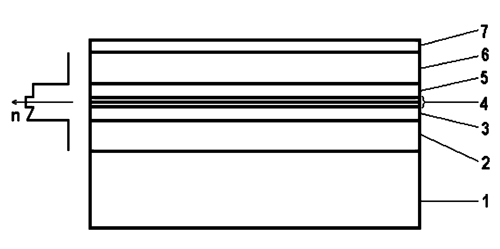
[0006] as attached figure 1 As shown, an asymmetric anti-waveguide large optical cavity semiconductor laser epitaxial structure includes a substrate 1, a lower confinement layer 2, a lower waveguide layer 3, a multi-quantum well active layer 4, an upper waveguide layer 5, an upper confinement layer 6 and an ohmic contact layer 7. The substrate 1 is the substrate for laser epitaxial growth; the material composition of the upper confinement layer 6 and the lower confinement layer 2 is uniform, and its main function is the optical confinement of the laser waveguide; the material composition of the upper waveguide layer 5 is uniform, and the thickness is 0.1-0.3 Micron, which is a P-type doped region, mainly provides the optical field waveguide and carrier barrier in the P-type region of the laser; the material composition of the lower waveguide layer 3 is a reverse linear gradient, with a thickness of 0.1-0.8 microns, close to the multi-quantum The material of the lower waveguid...


PUM


Abstract

The invention discloses an asymmetric inverse waveguide large optical cavity semiconductor laser structure, belonging to the technical field of semiconductor photo-electronic devices. Electro-optic efficiency and output power of the laser are limited as the known technology in the field is difficult to reduce series resistance and carrier leakage while reducing optical limiting factors of a laser waveguide, increasing effective waveguide width and reducing waveguide loss. The waveguide layer of the asymmetric inverse waveguide large optical cavity semiconductor laser adopts an asymmetric inverse linear graduated refractive index structure, so that the optical limiting factor of the laser waveguide is decreased efficiently, effective waveguide width is increased, carrier absorption loss and series resistance of the waveguide are reduced, and meanwhile the leakage of quantum well carriers is avoided. The technical scheme can be applied to manufacturing of various types of high-power semiconductor lasers.

Description

technical field [0001] The invention relates to an asymmetric anti-waveguide large optical cavity semiconductor laser structure, which belongs to the field of laser technology. Background technique [0002] The asymmetric large optical cavity semiconductor laser has the advantages of large waveguide width and small waveguide absorption. It is a typical epitaxial structure method for improving high-power semiconductor lasers, which is conducive to reducing the power density of the laser waveguide region and increasing the maximum output power level of the semiconductor laser. In the existing asymmetric large optical cavity semiconductor laser, the waveguide structure mainly adopts the uniform refractive index distribution structure of each layer, so that the increase of the effective waveguide width is limited, and the increase of the effective waveguide width mainly depends on the increase of the thickness of the lower waveguide layer and the increase of the refractive index....

Claims


Application Information

Patent Timeline
IPC IPC(8): H01S5/343
Inventor 薄报学高欣乔忠良张晶李辉李特曲轶
Owner CHANGCHUN UNIV OF SCI & TECH
Why Eureka
Try Eureka