Semiconductor drying device and method

A technology of drying device and drying method, applied in semiconductor/solid-state device manufacturing, heating device, drying and other directions, can solve problems such as lodging or adhesion, nano-pattern fracture, etc., and achieve the effect of eliminating surface tension

Inactive Publication Date: 2015-02-11
INST OF MICROELECTRONICS CHINESE ACAD OF SCI
View PDF3 Cites 5 Cited by
  • Summary
  • Abstract
  • Description
  • Claims
  • Application Information

AI Technical Summary

Problems solved by technology

[0005] The purpose of the embodiments of the present invention is to provide a semiconductor drying device and method, which breaks the cluster structure of water molecules on the s

Method used


Image

  • Semiconductor drying device and method
  • Semiconductor drying device and method
  • Semiconductor drying device and method

Examples


Embodiment 1

[0058] Embodiment 1: GHz electromagnetic wave drying width is the HSQ glue line of 14.9nm

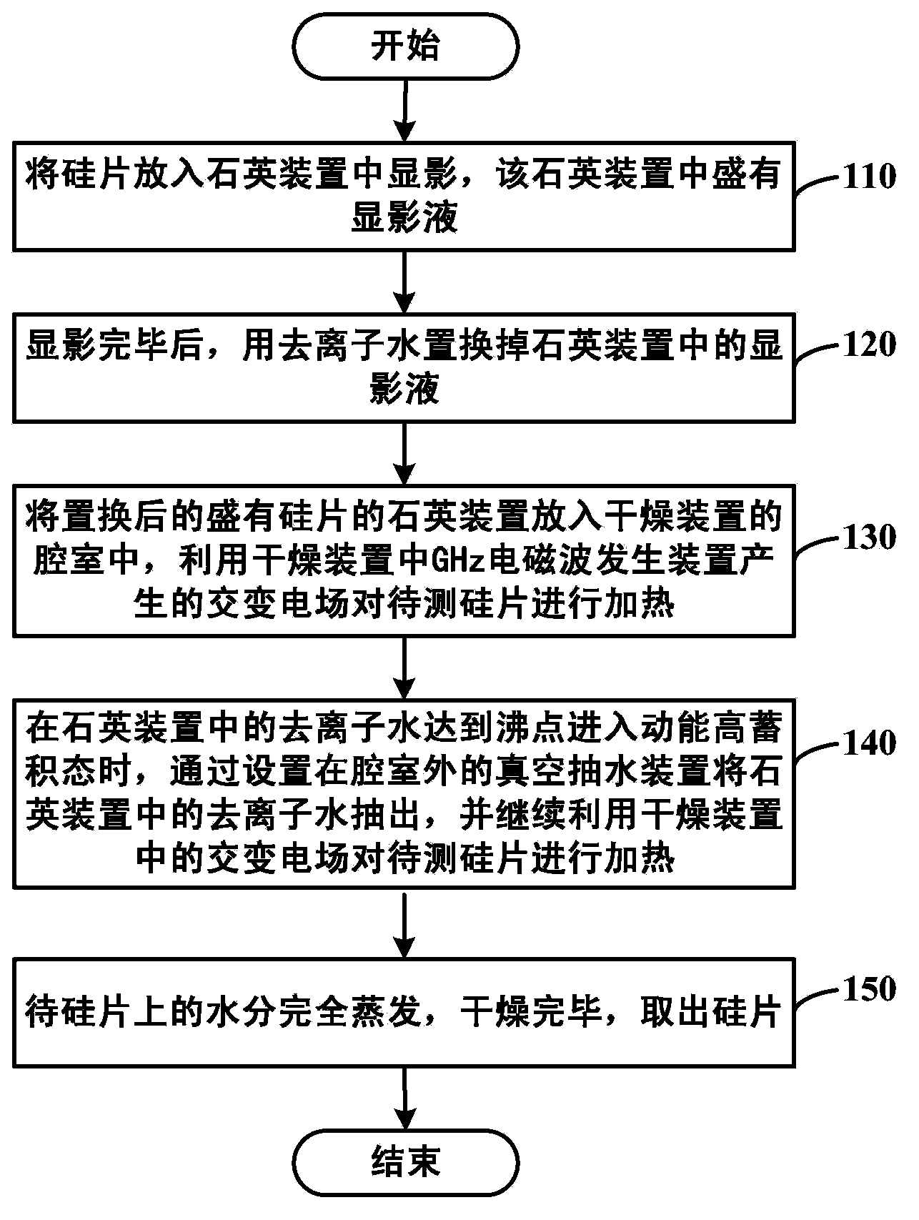
[0059] Step 1: Put 2, 4 or 8 silicon wafers with photoresist patterns into a quartz device for development, which has a developer suitable for HSQ glue;

[0060] Step 2: After the development is completed, replace the developer in the quartz device with deionized water;

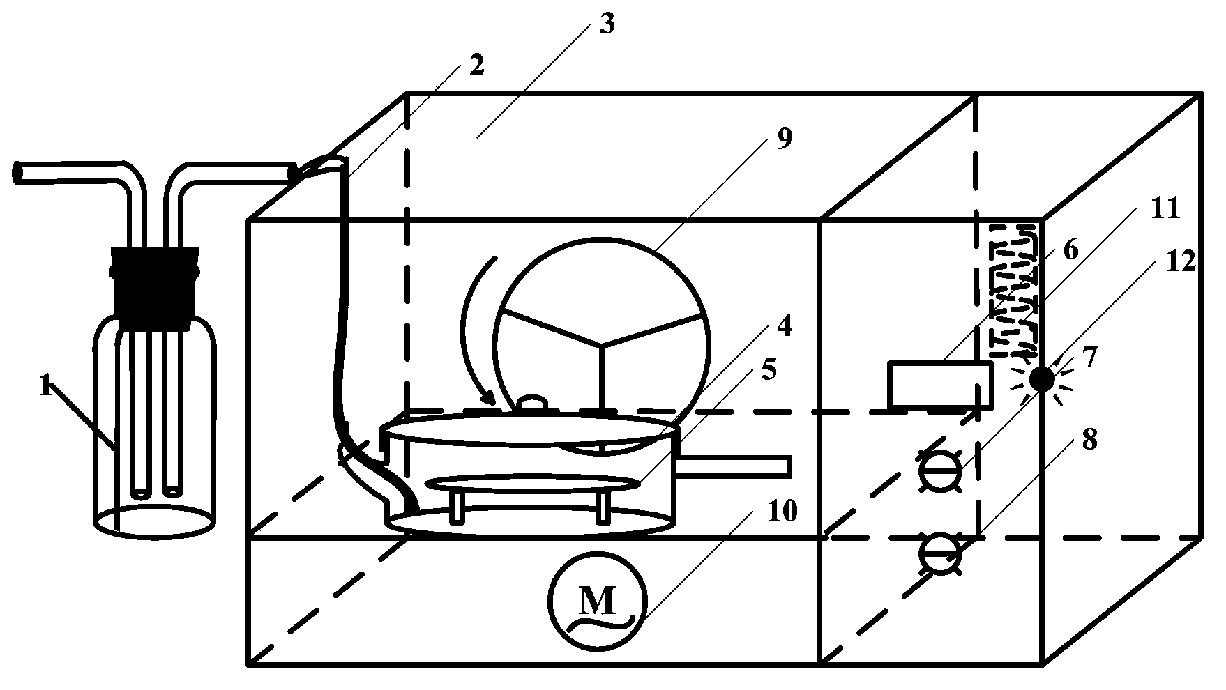
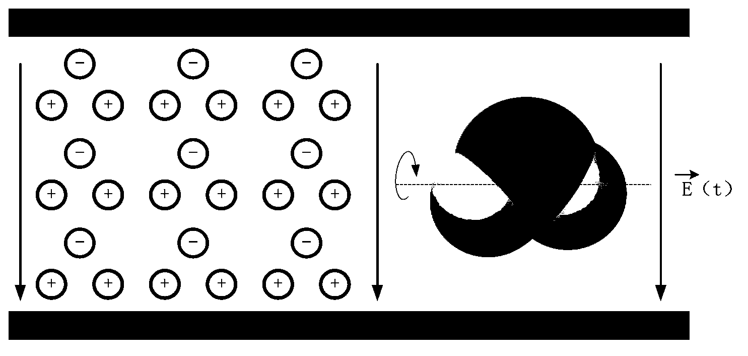
[0061] Step 3: Put the replaced quartz device with the silicon wafer in figure 1 In the chamber of the drying device shown, the alternating electric field in the drying device is used for heating. The specific heating principle is: water molecules are polar molecules, and as the direction of the alternating electric field changes rapidly, the polarity of the water molecules also changes. Then change the direction, when the changing frequency becomes faster and faster, the water molecules start to rotate at high speed, the kinetic energy increases, the friction and collision between the molecular clusters continue, the...


PUM


Abstract

The invention relates to the technical field of semiconductor, in particular to a semiconductor drying device. The drying device comprises a chamber, a quartz device and a GHz electromagnetic wave generation device, wherein the quartz device is arranged in the chamber for holding a silicon chip to be tested; the GHz electromagnetic wave generation device is arranged in the chamber for generating an alternating electric field to heat the silicon chip to be tested and increase the temperature of de-ionized water in the quartz device until water on the silicon chip to be tested is completely evaporated. The invention also provides a semiconductor drying method. By using the GHz electromagnetic wave generation device, electromagnetic wave generated by the GHz electromagnetic wave generation device enables the water to enter a high accumulation state of kinetic energy, so that a water cluster structure is broken, the surface tension of the water is eliminated, and the problems such as rupture, fall or adhesion of a nanometer graphic of a fine structure during drying are solved.

Description

technical field [0001] The invention relates to the technical field of semiconductors, in particular to a semiconductor drying device and method. Background technique [0002] In the fabrication process of microelectronic devices, with the further reduction of feature size and the further increase of structure complexity, the collapse of nano-device structures has become an increasingly serious problem. There are many reasons for the structure to collapse, such as being subjected to external forces, the stress of the structure itself, weaker structural materials, and surface tension during the drying process. Excluding other factors, the drying process becomes a very critical step. [0003] After cleaning the device with water as the main solvent, in the traditional drying method, the part with weak mechanical structure and the photoresist pattern with high aspect ratio will be damaged. Surface tension is a real problem during device drying after wet etch, because the surf...

Claims


Application Information

Patent Timeline
IPC IPC(8): H01L21/67F26B23/08
CPCH01L21/67115F26B23/04
Inventor 徐昕伟景玉鹏郭晓龙于明岩赵士瑞
Owner INST OF MICROELECTRONICS CHINESE ACAD OF SCI
Why Eureka
Try Eureka