Vacuum-processing apparatus, vacuum-processing method, and storage medium
A vacuum processing device and vacuum processing technology, applied in vacuum evaporation plating, manufacturing/processing of electromagnetic devices, ion implantation plating, etc., can solve the problems of reduced productivity, lack of stability of metal oxide film resistance, and metal oxide film resistance. Value instability and other problems, to achieve the effect of stable resistance value
- Summary
- Abstract
- Description
- Claims
- Application Information
AI Technical Summary
Problems solved by technology
Method used
Image
Examples
no. 2 Embodiment approach
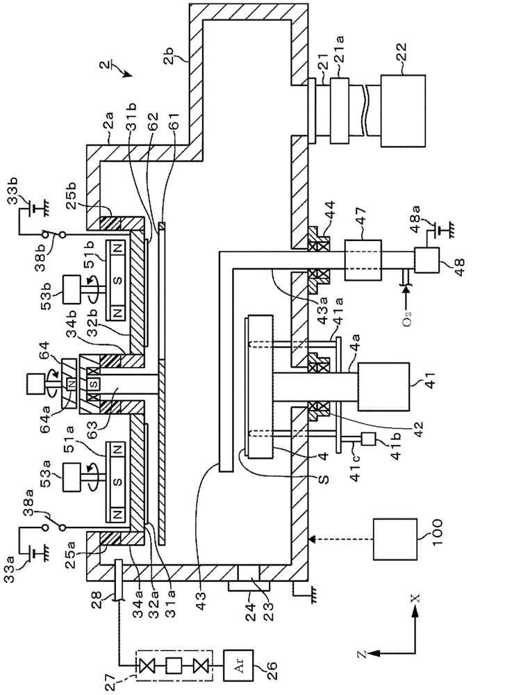
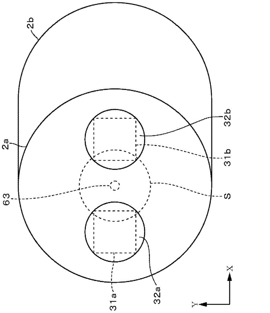
[0090] In the second embodiment to be described in detail below, the same reference numerals are attached to the same parts as those described in the above-mentioned first embodiment, and description thereof will be omitted. The second embodiment is as Figure 10 As shown, it is the common structure of the 1st target 31a and the 2nd target 31b in 1st Embodiment. In this case, the material of the target is a metal for forming a film on the substrate S and absorbs oxygen to form an oxide. Examples thereof include Hf, Mg, and alloys thereof.
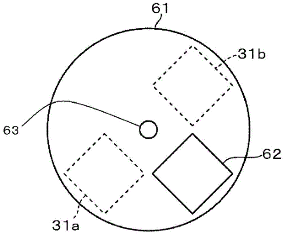
[0091] First, after loading the substrate S into the vacuum vessel 2, the flapper 61 is opened and the cover plate 43 is placed on the mounting portion 4. In this state, the target 31 is sputtered, and the particles of the target 31 are attached to the vacuum chamber. In the container 2, oxygen and moisture are absorbed. Next, the cover plate 43 is retracted from above the mounting part 4, and the target 31 is sputtered again, and target ...
Embodiment
[0094] (Example)
[0095] Using the apparatus of the above-mentioned embodiment, 25 silicon wafers were sequentially subjected to a metal oxide film-forming process, and the resistance value of the oxide film was measured on each of the obtained substrates, and the fluctuation of the resistance value was investigated. Specifically, under the conditions described in the embodiment, the thickness of the laminated 3 layers is MgO film.
[0096] Other conditions are as follows.
[0097] - Material of target 31a (absorbing member): Ti
[0098] ·Material of target 31b (film-forming material): Mg
[0099]・Diameter of substrate S: 300mm
[0100] The diameter of the cover plate 43: 450mm
[0101] - Voltage applied to the target electrode 32a: 380V
[0102] - Voltage applied to the target electrode 32b: 300V
[0103] · The distance between the substrate S and the targets 31a, 31b at the time of sputtering: 260mm
PUM
| Property | Measurement | Unit |
|---|---|---|
| thickness | aaaaa | aaaaa |
| thickness | aaaaa | aaaaa |
Abstract
Description
Claims
Application Information


