Al2O3/SiON inactivation layer structure of LED (light emitting diode) chip and growth method thereof

A technology of LED chip and growth method, which is applied in semiconductor/solid-state device manufacturing, electrical components, circuits, etc., can solve the problems of low density of passivation layer materials, small pinhole density, etc., achieve good compactness and reduce leakage , the effect of high crystal quality

Inactive Publication Date: 2015-02-18
GUANGDONG DELI PHOTOELECTRIC
View PDF6 Cites 7 Cited by
  • Summary
  • Abstract
  • Description
  • Claims
  • Application Information

AI Technical Summary

Problems solved by technology

[0004] Aiming at the deficiencies in the prior art, the present invention provides a novel Al 2 o 3 /SiON laminated structure passivation film and its growth method to solve the problem of low density of passivation layer material in the existing chip manufacturing process, the Al provided by the present invention 2 o 3 The /SiON passivation layer is a stacked structu

Method used


Image

  • Al2O3/SiON inactivation layer structure of LED (light emitting diode) chip and growth method thereof
  • Al2O3/SiON inactivation layer structure of LED (light emitting diode) chip and growth method thereof

Examples


Embodiment Construction

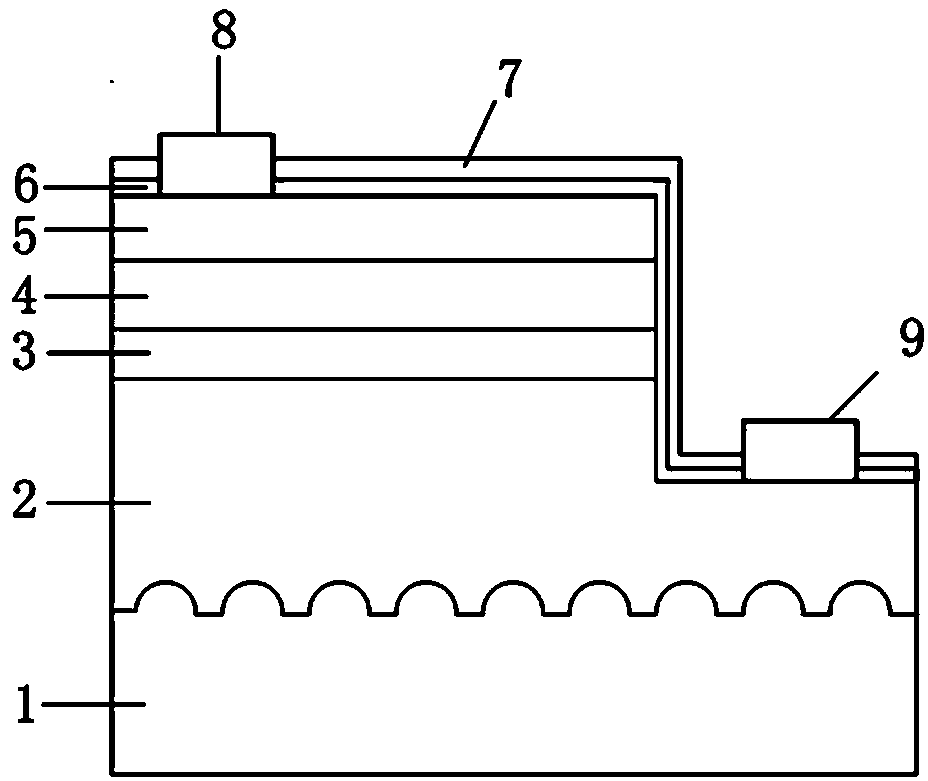
[0033] The specific embodiment of the present invention will be described in further detail below in conjunction with the accompanying drawings. The LP-MOCVD used in the examples is a self-made MOCVD equipment dedicated to growing oxide materials, and the model is SCMD-600B. The plasma-enhanced chemical vapor deposition PECVD used is commercially available The model sold is Plasmalab800Plus.

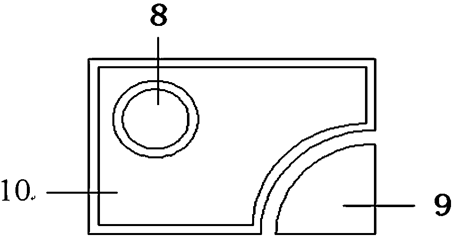
[0034] Such as figure 1 and figure 2 As shown, the Al of a kind of LED chip provided by the present invention 2 o 3 / SiON passivation layer structure, including pattern substrate 1, GaN-based epitaxial layer, ITO conductive film 5, P electrode 8, N electrode 9 and Al 2 o 3 / SiON composite layer 10, wherein the GaN-based epitaxial layer includes N-GaN2, quantum well MQW light-emitting layer 3 and P-GaN4, Al 2 o 3 / SiON composite layer 10 comprising Al 2 o 3 Passivation film 6 and SiON anti-reflection film 7. The manufacturing method of the above-mentioned embodiment is as follows:...


PUM


Abstract

The invention discloses an Al2O3/SiON inactivation layer structure of an LED (light emitting diode) chip. The Al2O3/SiON inactivation layer structure of the LED chip comprises an n type semiconductor layer, a luminous layer, a p type semiconductor layer and an ITO conducting layer, which are sequentially grown on a substrate, wherein an n type electrode is arranged on the n type semiconductor layer, and a p type electrode is arranged on the ITO conducting layer. The Al2O3/SiON inactivation layer structure of the LED chip is characterized in that Al2O3 layers and SiON layers are sequentially deposited on the upper surface of the chip on the outer sides of the n type electrode and the p type electrode. The Al2O3/SiON inactivation layer structure of the LED chip is of a lamination structure. A growth method of the Al2O3/SiON inactivation layer structure of the LED chip is a two step method, and includes: step one, using a self-manufactured LP-MOCVD device special for growth of oxide material to grow an Al2O3 film through a metal organic chemical sedimentation method which obtains good growth compactness for Al2O3 film material, obtains high crystalline quality, and can control growth velocity of the Al2O3 film well; step two, using a PECVD device to grow SiON film material. The Al2O3 film layer and the SiON film layer of the Al2O3/SiON inactivation layer structure of the LED chip respectively develop functions of electrode inactivation and a function of improving luminous efficiency of an antireflection film.

Description

technical field [0001] The present invention relates to the technical field of LED chips, in particular to an Al 2 o 3 / SiON passivation layer structure and its growth method. Background technique [0002] With the strong support of the government, light-emitting diode (LED) has become the mainstream product in the field of high-tech energy development. It has many advantages such as small size, long life (50,000 hours), high luminous efficiency, and energy saving. It has been widely used in in daily life. The surface of the LED chip is very sensitive to the external environment and will absorb other impurities to reduce the performance of the device. Therefore, it is often necessary to deposit a layer of insulating material on the surface of the chip to isolate the contact between the external environment and the chip surface and play a passivation role. In addition, the passivation layer also needs to function as an anti-reflection film to improve the light output effic...

Claims


Application Information

Patent Timeline
IPC IPC(8): H01L33/44H01L33/00H01L21/205
CPCH01L21/205H01L33/005H01L33/44H01L2933/0025
Inventor 王波郝锐叶国光易翰翔李方芳
Owner GUANGDONG DELI PHOTOELECTRIC
Why Eureka
Try Eureka