Manufacturing method of thick hole copper PCB

A manufacturing method and thick-hole copper technology, applied in multilayer circuit manufacturing, printed circuit manufacturing, circuit metal processing, etc., can solve problems affecting PCB quality, stretching, etc., to improve production efficiency, reduce thickness, and benefit The effect of etching

Active Publication Date: 2015-02-18
JIANGMEN SUNTAK CIRCUIT TECH
View PDF5 Cites 17 Cited by
  • Summary
  • Abstract
  • Description
  • Claims
  • Application Information

AI Technical Summary

Problems solved by technology

[0003] The present invention aims at the problem that in the production of the existing copper PCB with thick holes, the surface copper thickness is too thick or the semi-finished product is stretched by abrasive belt grinding, which affects the quality of the PCB. Method for making over-thick thick-hole copper PCB

Method used


Image

  • Manufacturing method of thick hole copper PCB

Examples


Embodiment 1

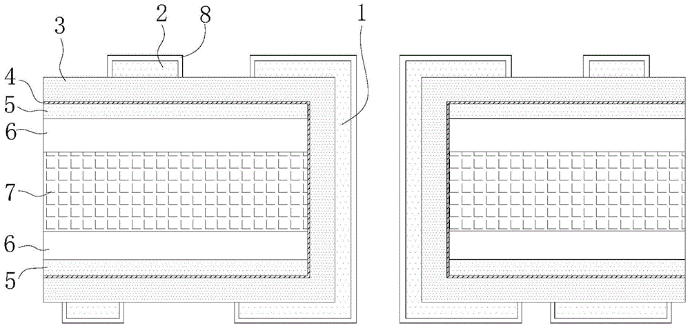
[0016] This embodiment provides a method for making a thick hole copper PCB. After using this method to carry out pattern electroplating on the multilayer board, the structure of the multilayer board is as follows: figure 1 shown.

[0017] Wherein, the parameters of the manufactured PCB are as follows.

[0018] Finished plate thickness: 2.0mm; completed minimum hole diameter: 0.25mm; thickness-to-diameter ratio: 8:1; thickness of the copper layer on the hole wall ≥ 60μm; minimum line width / line spacing: 0.2 / 0.2mm.

[0019] The specific production steps are as follows:

[0020] (1) Pressing to form a multi-layer board

[0021] First, as in the PCB production process of the prior art, the PCB raw material is cut to obtain the core board 7, and then the inner layer pattern is transferred on the core board 7 to form the inner layer circuit circuit, and then the core board 7 and the outer layer are connected through the prepreg 6 The copper foils are pressed together to form a m...


PUM

PropertyMeasurementUnit
Thicknessaaaaaaaaaa

Abstract

The invention relates to the technical field of PCB production, in particular to a manufacturing method of a thick hole copper PCB. The method is characterized in that a board electric copper layer is formed on a hole wall through whole board electroplating, a thickened copper layer is further formed in the hole wall through pattern electroplating during outer-layer circuit manufacturing, and the thickened copper layer and the board electric copper layer jointly form a hole wall copper layer. The method has the advantages that abrasive belt board grinding in film hole plating is omitted, accurate alignment of subsequent work procedures is unaffected due to the fact stretching of a semi-finished product is avoided, and production efficiency can be increased; due to the fact that the part of the copper thickness of the hole wall copper layer is formed during pattern electroplating, the problems that film clamping is caused by the fact that the copper layer on the surface of a multilayer board is excessively thick, and unclean etching occurs are solved; outer layer copper coil thickness is reduced before drilling, surface copper thickness can be reduced relatively, and etching is benefited.

Description

technical field [0001] The invention relates to the technical field of PCB manufacturing, in particular to a method for manufacturing a thick-hole copper PCB. Background technique [0002] With the rapid development of electronic and communication products, the amount of signal transmission increases and the transmission speed accelerates, which makes the design of PCB move towards the direction of high frequency, high power and miniaturization. Copper degree and hole copper thickness (hole wall copper thickness of metallized hole) put forward higher requirements. In the industry, the production of thick-hole copper PCBs (that is, PCBs with metallized holes with copper thickness ≥ 60 μm) usually adopts the following two operating methods: 1. Film plated hole process: use a dry film and open at the metallized hole For windows, first electroplate copper on the hole wall, then use abrasive belt grinding to remove the protruding copper at the hole, then do a second dry film, an...

Claims


Application Information

Patent Timeline
IPC IPC(8): H05K3/00
CPCH05K3/46H05K2203/03H05K2203/0703
Inventor 敖四超韦昊刘松伦邓峻
Owner JIANGMEN SUNTAK CIRCUIT TECH
Why Eureka
Try Eureka