Heating bearing platform of laser annealing machine table

A technology of carrying platform and laser annealing, which is used in the manufacture of electrical components, electric solid-state devices, semiconductor/solid-state devices, etc. Effect

Inactive Publication Date: 2015-02-25
SHANGHAI HUALI MICROELECTRONICS CORP
View PDF4 Cites 2 Cited by
  • Summary
  • Abstract
  • Description
  • Claims
  • Application Information

AI Technical Summary

Problems solved by technology

because figure 1 The heating bearing platform 2 of the existing laser annealing machine is in the form of overall uniform temperature heating, and the heat dissipation temperature loss in the edge area of ​​the silicon wafer is greater than that in the central area, causing the temperature in the edge area of ​​the silicon wafer to be about 5-5% lower than that in the central area. around 7℃

Method used


Image

  • Heating bearing platform of laser annealing machine table
  • Heating bearing platform of laser annealing machine table
  • Heating bearing platform of laser annealing machine table

Examples


Embodiment Construction

[0028] The specific embodiment of the present invention will be further described in detail below in conjunction with the accompanying drawings.

[0029] It should be noted that, in the following specific embodiments, when describing the embodiments of the present invention in detail, in order to clearly show the structure of the present invention for the convenience of description, the structures in the drawings are not drawn according to the general scale, and are drawn Partial magnification, deformation and simplification are included, therefore, it should be avoided to be interpreted as a limitation of the present invention.

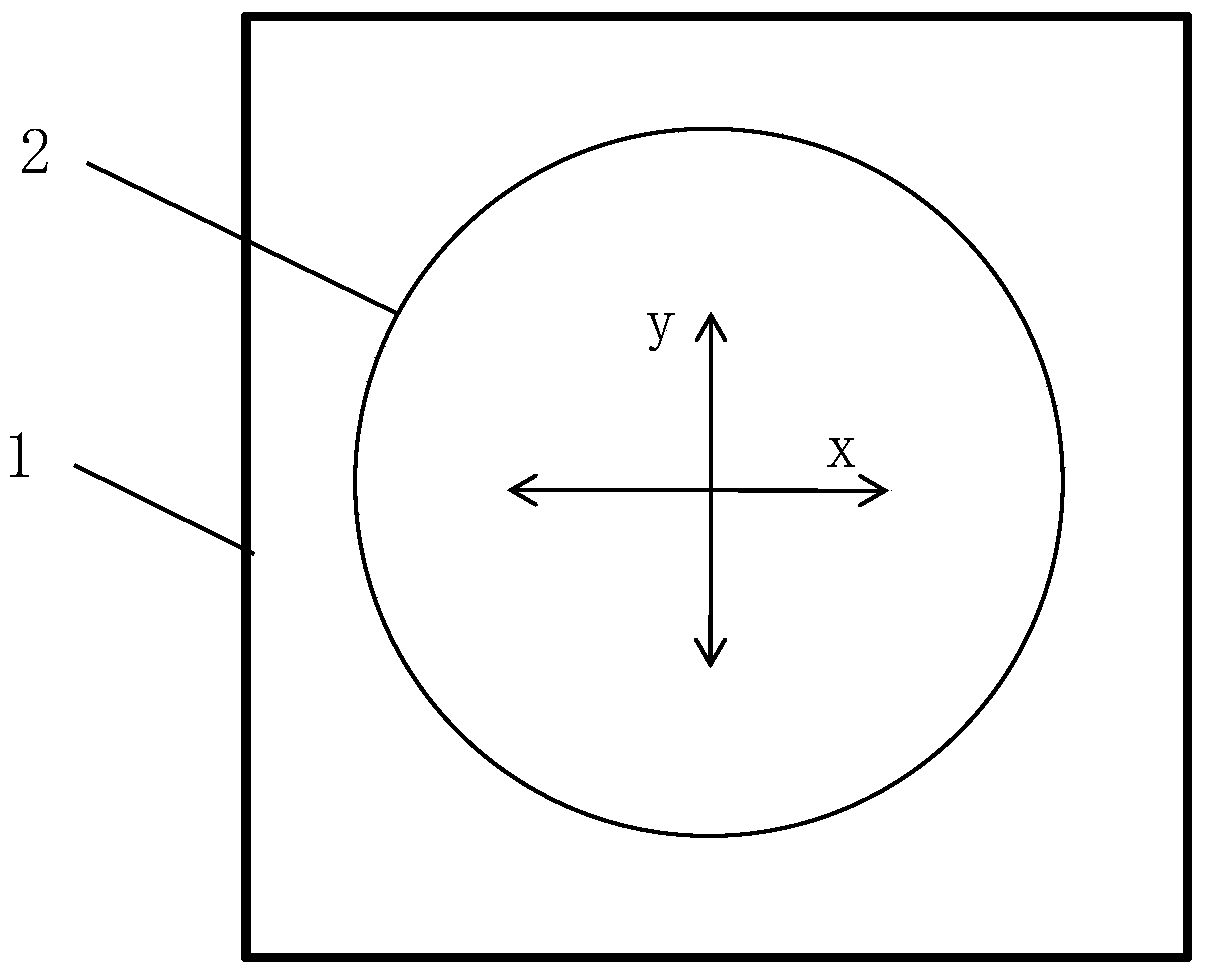
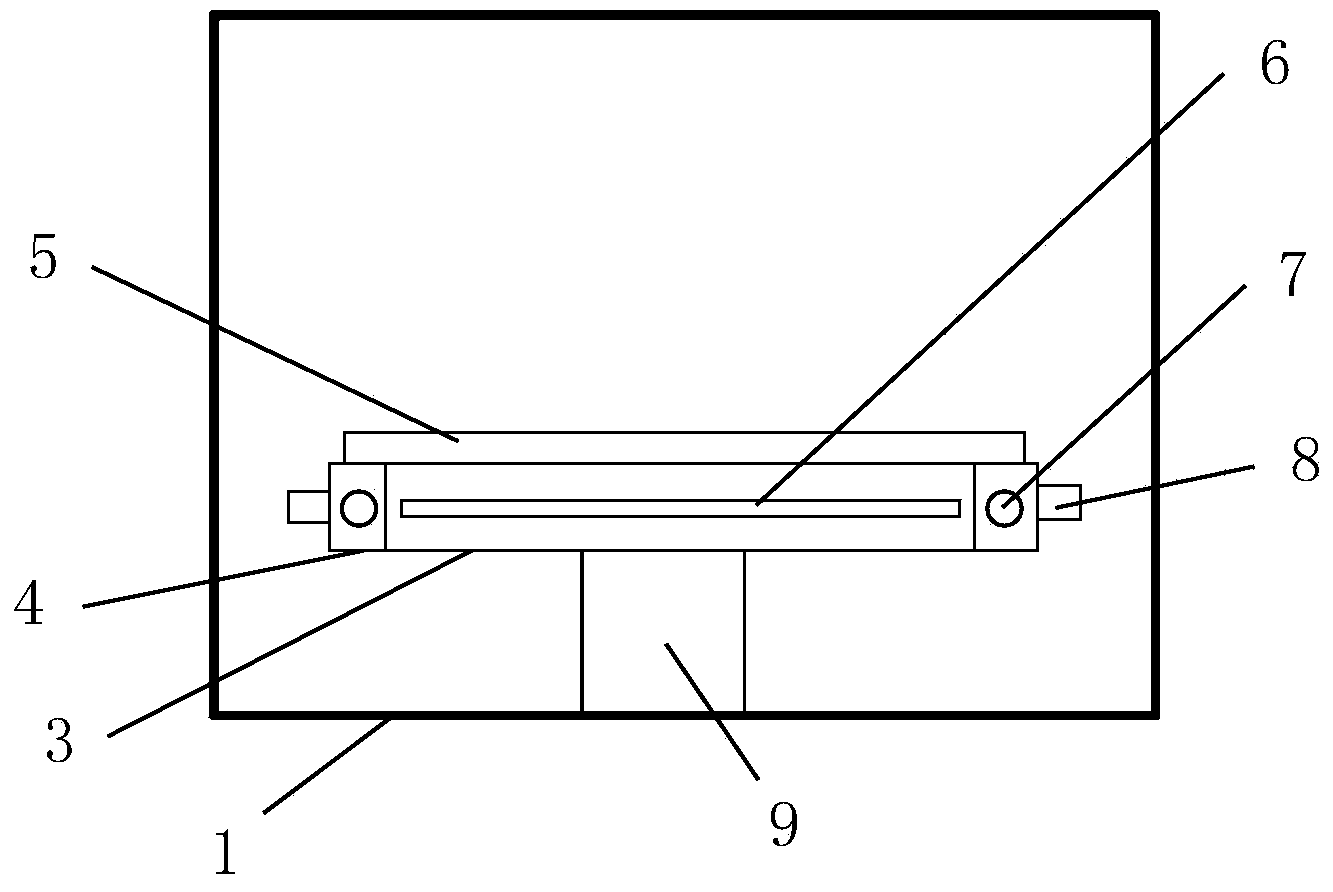
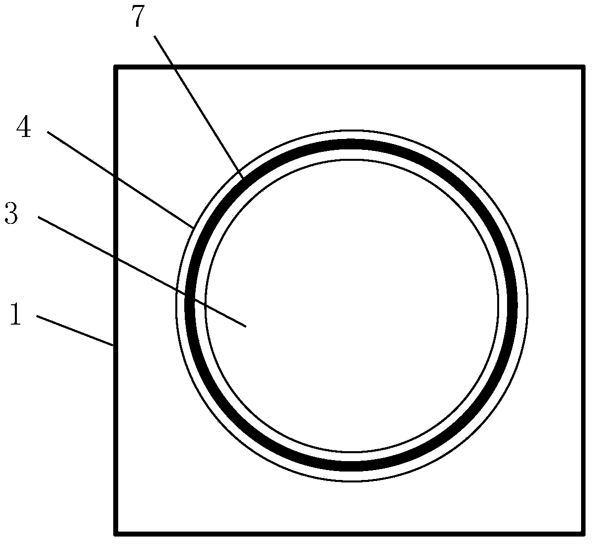
[0030] In order to facilitate the understanding of the present invention, the structure of the process chamber of the existing laser annealing machine is firstly described. see figure 1 , figure 1 It is a top view schematic diagram of the structure of a process chamber of an existing laser annealing machine. Such as figure 1 As shown, a ceramic h...


PUM


Abstract

The invention discloses a heating bearing platform of a laser annealing machine table. A synchronously-moving combined heating bearing platform body is formed by arranging a second heating bearing platform body on the periphery of a first heating bearing platform in a surrounding mode. Heating is independently carried out through heating units arranged on the first heating bearing platform body and the second heating bearing platform body respectively, the heating temperature of the second heating bearing platform body is higher than that of the first heating bearing platform body, the heat dissipation temperature loss of a silicon wafer edge area borne by the first heating bearing platform body and the second heating bearing platform body can be offset, the preheating temperature of the silicon wafer edge area is increased, and therefore the phenomenon that when the laser annealing technology is carried out, the square resistance value is relatively high due to the low silicon wafer edge temperature is eliminated, and the improvement of the on-chip resistance in a silicon wafer and the overall device performance are improved.

Description

technical field [0001] The invention relates to the field of semiconductor manufacturing equipment, more specifically, to a combined heating and bearing platform used in a laser annealing machine to improve the uniformity of resistance at the edge of a silicon wafer. Background technique [0002] In the manufacture of semiconductor integrated circuits, according to different processes, such as including (but not limited to) chemical vapor deposition, oxidation or nitriding, ion implantation annealing, and doping activation, it is often necessary to perform multi-step annealing on the wafer. Heat treatment repairs crystal damage and eliminates dislocations. [0003] With the technological evolution of large-scale integrated circuits, after entering the 40nm node, the requirements for junction depth are becoming shallower and shallower. Therefore, the Spike Anneal (Spike Anneal) process traditionally used to activate source / drain dopant elements after ion implantation is no l...

Claims


Application Information

Patent Timeline
Patent Type & Authority Applications(China)
IPC IPC(8): H01L21/683
CPCH01L21/683H01L2221/683
Inventor 邱裕明肖天金曹文杰
Owner SHANGHAI HUALI MICROELECTRONICS CORP
Why Eureka
Try Eureka