LDMOS capable of lowering LDMOS on resistance and increasing breakdown voltage in on state

A technology of semiconductors and oxide semiconductors, applied in circuits, electrical components, semiconductor devices, etc., can solve problems such as low breakdown voltage and breakdown, and achieve the effect of reducing on-resistance and increasing breakdown voltage

Inactive Publication Date: 2015-02-25
CSMC TECH FAB1
View PDF4 Cites 0 Cited by
  • Summary
  • Abstract
  • Description
  • Claims
  • Application Information

AI Technical Summary

Problems solved by technology

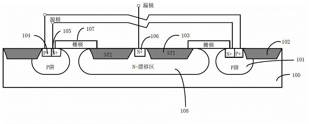
In the prior art, in order to obtain a smaller on-resistance, the size of the drift region is made small. When the LDMOS is working under high-voltage conditions, the depletion layer in the drift region extends to the drain, and it is easy to expand to a high concentration in the drain region. The lead-out end (such as n+), thus forming a large electric field at the boundary of the high-concentration lead-out end, it is easy to cause breakdown due to impact ionization caused by the large electric field, that is, the breakdown voltage in the on state is low

Method used


Image

  • LDMOS capable of lowering LDMOS on resistance and increasing breakdown voltage in on state
  • LDMOS capable of lowering LDMOS on resistance and increasing breakdown voltage in on state
  • LDMOS capable of lowering LDMOS on resistance and increasing breakdown voltage in on state

Examples


Embodiment Construction

[0019] In the following description, numerous specific details are given in order to provide a more thorough understanding of the present invention. It will be apparent, however, to one skilled in the art that the present invention may be practiced without one or more of these details. In other examples, some technical features known in the art are not described in order to avoid confusion with the present invention.

[0020] In order to thoroughly understand the present invention, detailed steps will be presented in the following description, so as to explain how the present invention improves the process of fabricating semiconductor device structures to solve the problems in the prior art. Obviously, the practice of the invention is not limited to specific details familiar to those skilled in the semiconductor arts. Preferred embodiments of the present invention are described in detail below, however, the present invention may have other embodiments besides these detailed d...


PUM


Abstract

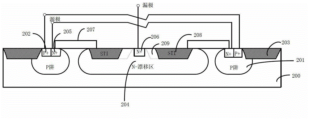
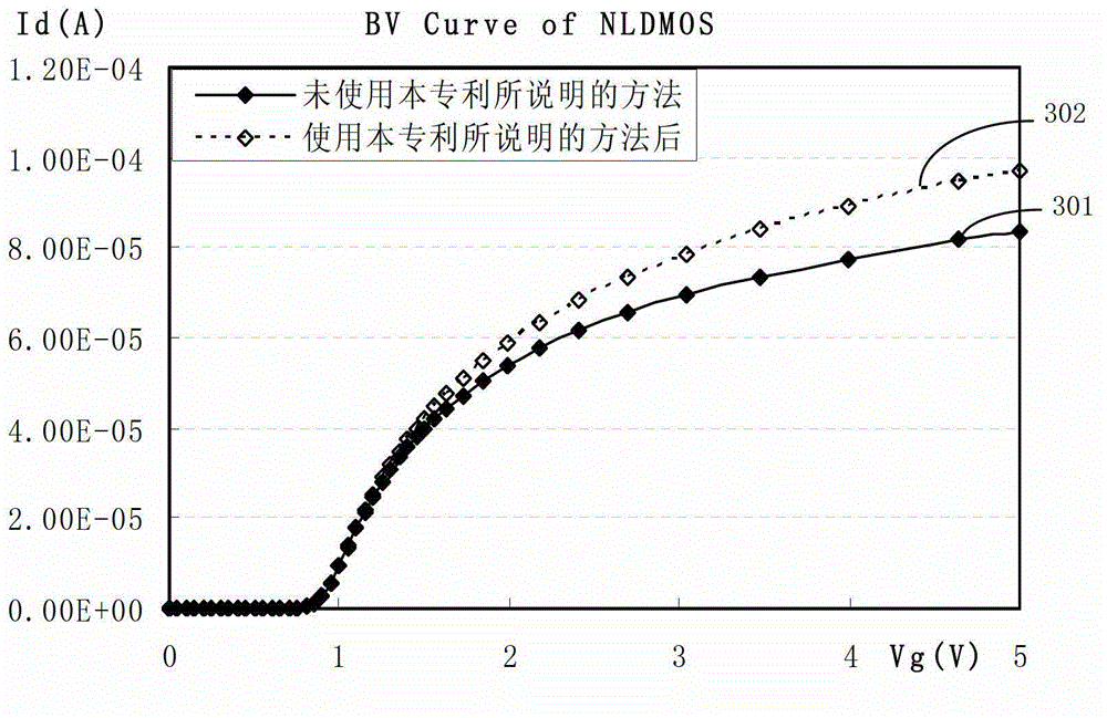
A laterally double-diffused metal-oxide-semiconductor field effect transistor, comprising: a semiconductor substrate (200), located in a body area (201) for said semiconductor substrate (200); a drift region (204), located in said semiconductor substrate (200); a source region (205) and a body lead-out region (202) located in the body region (201) and separated from the drift region (204); a field region (208) and a drain region (206) located in the drift region (204); and a gate electrode located on the surface of the semiconductor substrate (200), partially covering the body region (201), the drift region (204) and the field region (208). The field region (208) and drain region (206) are separate one from the other by a certain distance. In the present semiconductor component, while the original dimensions of the drift region (204) remain unchanged, the dimensions of the field region (208) of the drift region (204) near the drain end are shortened, changing the drift region, which originally was wholly a field region, into one section of field region and one section of active region, thus reducing LDMOS on-resistance, while at the same time increasing on-state breakdown voltage.

Description

technical field [0001] The invention relates to the technical field of lateral double diffused metal oxide semiconductor field effect transistors (Lateral Double Diffused MOSFET, LDMOS), in particular to an LDMOS device structure that reduces the on-resistance and simultaneously increases the on-state breakdown voltage. Background technique [0002] With the continuous development of semiconductor technology, lateral double-diffused metal-oxide-semiconductor field-effect transistor (LDMOS) devices are widely used in mobile phones, especially in cellular phones, due to their good short-channel characteristics. With the continuous increase of the mobile communication market (especially the cellular communication market), the manufacturing process of LDMOS devices is becoming more and more mature. As a power switching device, LDMOS has the characteristics of relatively high working voltage, simple process, and easy process compatibility with low-voltage CMOS circuits. It includ...

Claims


Application Information

Patent Timeline
IPC IPC(8): H01L29/78H01L29/06
CPCH01L29/7835H01L29/0653H01L29/1045H01L29/66659H01L29/7816H01L29/06
Inventor 韩广涛孙贵鹏黄枫
Owner CSMC TECH FAB1
Why Eureka
Try Eureka