Doping structure for improving efficiency and bandwidth of silicon-based electro-optic tuning device

A silicon-based and device technology, applied in the field of doped structures, can solve the problems of difficulty in taking into account modulation efficiency and modulation rate, and achieve the effects of improving intrinsic electrical bandwidth, reducing costs, and improving tuning efficiency

Active Publication Date: 2015-03-04
WUHAN POST & TELECOMM RES INST CO LTD
View PDF4 Cites 33 Cited by
  • Summary
  • Abstract
  • Description
  • Claims
  • Application Information

AI Technical Summary

Problems solved by technology

[0013] The technical problem to be solved by the present invention is to overcome the problem that the silicon-based electro-o

Method used


Image

  • Doping structure for improving efficiency and bandwidth of silicon-based electro-optic tuning device
  • Doping structure for improving efficiency and bandwidth of silicon-based electro-optic tuning device
  • Doping structure for improving efficiency and bandwidth of silicon-based electro-optic tuning device

Examples


Embodiment Construction

[0041] The present invention will be described in detail below in conjunction with the accompanying drawings and specific embodiments.

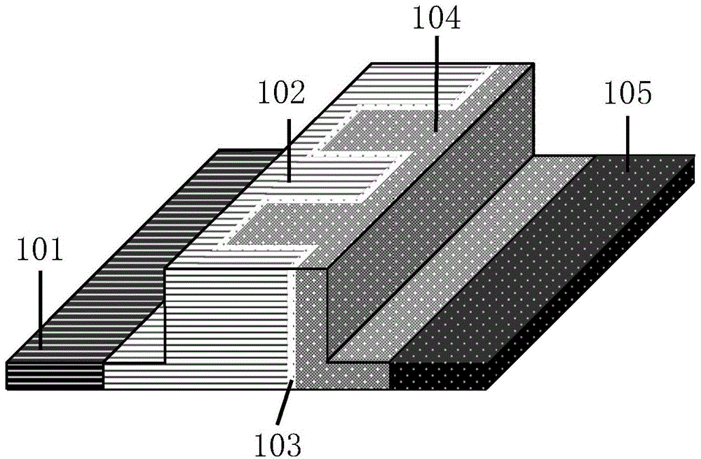
[0042] Such as figure 1 As shown, the present invention provides a doped structure that improves the efficiency and bandwidth of silicon-based electro-optical tuning devices. The doped structure is poured on an active silicon-based ridge-type optical waveguide through ion implantation and rapid thermal annealing process. The material of the active silicon-based ridge optical waveguide is usually SOI (silicon-on-insulator, silicon on insulating substrate) wafer, the height of the inner ridge is between 300nm and 600nm (including 300nm and 600nm), and the height of the outer ridge is The height is lower than the inner ridge height; processed by inductively coupled plasma etching (ICP), by reactive ion etching (RIE), wet etching or thermal oxidation.

[0043] The doping structure includes:

[0044] The P+ type doped region 101 is arranged on o...


PUM

PropertyMeasurementUnit
Thicknessaaaaaaaaaa

Abstract

The invention discloses a doping structure for improving efficiency and bandwidth of a silicon-based electro-optic tuning device. The doping structure comprises a P+ type doping area arranged on the outer ridge area on one side close to the edge and is in ohmic contact with the above metal; A P type doping area is arranged on the outer ridge area connected with the P+ type doping area and extends to the inner ridge area; An N+ type doping area is arranged on the outer ridge area on the other side close to the edge and is in ohimic contact with the above metal; A N-type doping area is arranged on the outer ridge area connected with the N+ type doping area and extends to the inner ridge area and is complementary with the P type doping area; An almost-I type doping area is arranged between the P type doping area and the N type doping area and forms an almost PIN knot with the P type doping area and the N type doping area. By means of the doping structure, the silicon-based electro-optic tuning device is improved in the aspects of the modulator speed, efficiency and insertion loss, the cost is reduced, the requirement of the ion implantation process for the mask alignment accuracy is reduced, and large-scale manufacture of the device is facilitated.

Description

technical field [0001] The invention relates to a silicon-based electro-optic modulator in the field of optical communication, in particular to a doping structure for improving the efficiency and bandwidth of a silicon-based electro-optic tuning device. Background technique [0002] In optical communication systems, tunable silicon-based optical waveguides are key optical components and can be used in active optical core devices such as optical modulators, optical switches, routers, tunable optical attenuators, and wavelength tunable filters and lasers. Among them, the high-speed optical modulation function of tunable silicon-based optical waveguides is usually based on the high-speed silicon-based electro-optic effect. [0003] Pure unstrained silicon single crystal is a kind of crystal with central inversion symmetry, so there is no linear electro-optic effect (Pockels effect) in this silicon single crystal, while the second-order electro-optic effect of silicon (Kerr effe...

Claims


Application Information

Patent Timeline
IPC IPC(8): H01L33/14G02F1/035
CPCG02F1/035H01L33/02H01L33/14G02F1/025
Inventor 肖希李淼峰王磊邱英杨奇余少华
Owner WUHAN POST & TELECOMM RES INST CO LTD
Why Eureka
Try Eureka