Wavelength-tunable double-ring structure plasmonic laser based on metamaterial antenna
A plasmonic and metamaterial technology, applied in the field of lasers, can solve the problems of device miniaturization, and achieve the effects of easy integration, high tuning rate, high speed and high efficiency tuning
- Summary
- Abstract
- Description
- Claims
- Application Information
AI Technical Summary
Problems solved by technology
Method used
Image
Examples
Embodiment 1
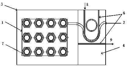
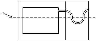
[0032] designed as figure 1 The laser structure shown, the metallic split-ring resonator structure as Figure 7 shown in d. The material of the top patch antenna 1 is gold, the size is 0.63 mm * 0.45 mm, and the thickness is 100 nanometers; the material of the metal transmission line 2 is gold, and the width is 0.29 mm; the material of the metamaterial antenna dielectric layer 3 is FR4, and the thickness is 200 microns; the laser The cladding material of the resonant cavity 4 is PTFE with a thickness of 200 microns; the thickness of the silicon substrate 5 is 100 microns; the material of the metal substrate layer 64 of the SIMS waveguide is gold with a thickness of 200 nanometers; the material of the metal strip 63 is gold with a thickness of 200 nanometers; the dielectric strip contains 62, and the material is doped Er 3+ SiO 2 Material, the thickness is 5 nanometers; Si strip 61, thickness is 200 nanometers; Metal strip 63, dielectric strip 62, Si strip 61 have a width of...
Embodiment 2
[0034] designed as figure 1 The laser structure shown, the metallic split-ring resonator structure as Figure 7 as shown in c. The material of the top patch antenna 1 is gold, and the size is 63 microns*45 microns; the material of the metal transmission line 2 is gold, and the width is 26 microns; the material of the metamaterial antenna dielectric layer 3 is FR4, and the size is 160 microns; the laser cavity cladding 4 The material is PCTFE with a size of 160 microns; the thickness of the silicon substrate 5 is 100 microns; the material of the metal substrate layer 64 of the SIMS waveguide is gold, and the thickness is 200 nanometers; the material of the metal strip 63 is gold, and the thickness is 200 nanometers; 62, the material is doped Er 3+ SiO 2 Material, the thickness is 5 nanometers; Si strip 61, the thickness is 200 nanometers; the width of metal strip 63, dielectric strip 62, and Si strip 61 is 100 nanometers, and the radius of the ring resonant cavity is 500 nan...
PUM
| Property | Measurement | Unit |
|---|---|---|
| thickness | aaaaa | aaaaa |
| thickness | aaaaa | aaaaa |
| thickness | aaaaa | aaaaa |
Abstract
Description
Claims
Application Information


